Laboratory
At UCLA, we have a world-class facility for conducting research in chemical vapor deposition and plasma processing. Moreover, our people are just outstanding! You cannot find a better place to obtain a Ph.D. degree in the exciting field of semiconductor manufacturing.
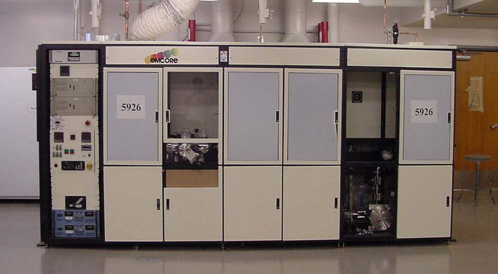
Check out our new MOCVD reactor for research on manufacturing InP optoelectronic integrated circuits:
Click on the links below to learn more about our program.
Group Members | |
Facilities | |
Sponsors |
Awards | |
Recent Graduates |
Nanoelectronics Research Facility | |
Semiconductor Curriculum |