198th Electrochemical Society Meeting
MISFIT DISLOCATION NUCLEATION STUDY IN P/P+ SILICON
Petra Feichtinger1, Mark S. Goorsky1,
Dwain Oster2, Tom D'Silva2, and Jim Moreland3
1 Dept. Materials Science and Engineering UCLA, Los Angeles, CA
90025.
2 Wacker Siltronic Corp. Portland, OR 97210.
3 Wacker Siltronic AG 84489 Burghausen, Germany
A potential problem related with the p/p+ structure is that
high boron concentrations reduce the lattice parameter of silicon.1
Therefore, lightly doped epitaxial layers are compressively strained with
respect to the substrate and this strain can foster the formation of interfacial
misfit dislocations. This issue of strain relaxation becomes more problematic
with the industry push to lower resistivity substrates.
We studied misfit dislocation generation sites in epitaxial p/p+ silicon wafers.
These strain-relaxing defects nucleate heterogeneously at stress concentrators
at the lattice-mismatched interface. Different kinds of possible stress concentrators
have been identified to act in strained epilayer systems. In SiGe/Si, they
include b-SiC precipitates (due to insufficient
substrate cleaning)2, Ge-rich platelets2, oxide particles3,
diamond defects4, trace impurities of copper5, and crystal
defects at the wafer edges6. For III-V semiconductors, it has been
shown7 that highly dense threading dislocations in the substrate
bow out in the interface to form interfacial misfit dislocations in order
to relieve the misfit stress.
For hyper pure epitaxial silicon grown by highly clean CVD at very high temperature
(~ 1100 °C), most of these conditions do not apply. The threading dislocation
density is very small and particle contamination is extremely low. The wafer
edges have been shown to act as misfit dislocation nucleation sites in p/p+
silicon.8 Thus a challenge in the fabrication of defect free large
diameter silicon wafers for power MOS applications is the reduction of crystal
imperfections around the wafer edges.
We examined the effect of a variation of wafer edge treatments on misfit dislocation
formation in p/p+ silicon test wafers. The misfit in this system is low (~
1.6 * 10-4) compared to other strained epitaxial systems. The samples
were 150 mm Czochralski grown wafers with high boron doping level ([B] ~ 3*1019
cm-3). Differing treatments were used during the processing of
the test wafers to create a variation of mechanical damage around the substrate
wafer edges. A measure for the mechanical damage around the wafer edges was
gained using a profilometer. Nominally boron doped epitaxial layers ([B] ~
1*1015 cm-3) beyond the critical thickness were deposited
by vapor phase epitaxy at ~ 1100 °C in a single wafer reactor. The influence
of the residual crystalline damage around the test wafer edges on the appearance
of misfit dislocation segments was studied. Double crystal x-ray topography
was used to visualize the misfit dislocation segments around the wafer periphery.
The use of a curved first crystal allows the imaging of a large sample area
with uniform curvature.9
Figure 1 shows double crystal x-ray topographs of one series of test wafers.
Figure 2 shows a graph of the measured data. As the roughness around the wafer
edge decreases, the misfit dislocation length and density decrease as well.
The total misfit dislocation length across the whole wafer decreases from
~ 20 m to ~ 0.1 m as the edge gets smoother.
We have shown that the wafer edge shaping and subsequent damage removal steps
determine the residual damage around the wafer edges, which during epitaxial
layer growth may act as misfit dislocation nucleation sites if not removed
prior to epitaxy. Edge treatments lowering the wafer edge roughness exhibit
a great reduction (<10 cm-1) or even the absence of misfit dislocations
compared to untreated edges (~1000 cm-1).
References:
1. H. Holloway and S. L. McCarthy, J. Appl. Phys. 73, 103 (1993).
2. D. D. Perovic and D. C. Houghton, Mat. Res. Soc. Symp. Proc. 263,
391 (1992).
3. C. G. Tuppen, C. J. Gibbings, and M. Hockley, J. Cryst. Growth 94,
392-404 (1989).
4. D. J. Eaglesham, E. P. Kvam, D. M. Maher, C. J. Humphreys, and J. C. Bean,
Phil. Mag. 59, 1059 (1989).
5. V. Higgs, P. Kightley, P. J. Goodhew, and P. D. Augustus, Appl. Phys. Lett.
57, 829 (1991).
6. M. Albrecht, S. Christiansen, J. Michler, W. Dorsch, H. P. Strunk, et al.,
Appl. Phys. Lett. 67, 1232 (1995).
7. J. W. Matthews and A. E. Blakeslee, J. Crystal Growth 27, 118-125
(1974).
8. H. Fukuto, P. Feichtinger, M. S. Goorsky, T. Magee, D. Oster, J. Moreland,
et al., J. Crystal Growth 209, 716 (2000).
9. M. S. Goorsky, P. Feichtinger, H. Fukuto, and G. U'Ren, Phil. Trans. R.
Soc. Lond. A 357, 2777 (1999).
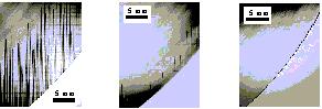
Figure 1. Double crystal topographs taken at the wafer periphery of test
wafers. A difference in misfit dislocation density and length around the wafer
periphery depending on the roughness as a measure of residual damage around
the wafer edge is clearly visible.
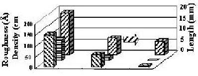
Figure 2. Measured misfit dislocations length (mm), misfit dislocation
density (cm-1), and roughness data (Å) quantifying the double crystal topographs
in Figure 1.