|
Organize by EPA Centre, University
of California, Los Angeles, City
University of Hong Kong
Training Course on
Reliability of Pb-free Solder Joint
in Advanced Electronic Packaging
Technology
The rapid growth in wireless, portable, and
multi-functional devices has enhanced the development of electronic
packaging technology.?There is a
greater demand of flip chip assembly in advanced packaging, especially the
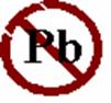
use of?Pb-free solder joints.?European Union Congress has a ban on
Pb-based solders in consumer electronic products on July 1st,
2006.?The reliability of Pb-free
solder joins is of concern in manufacturing industry.?For example, the reflow of Pb-free solder
paste produces many more residue voids than SnPb solder paste.?This one-day course will start from the
trend in electronic packaging technology.?
It will be followed by the analysis of solder reactions in wetting
and in solid state aging.?The unique
reliability behavior of spalling of intermetallic compounds in thin film
under-bump-metallization and the formation of Kirkendall voids in thick
under-bump-metallization will be discussed.?
Next, electromigration induced failure in flip chip solder joints
will be analyzed.?The unique failure
mode of electromigration in flip chip solder joints will be explained on
the basis of current crowding.?Joule
heating that leads to melting of flip chip solder joints will be discussed.?Thermomigration in solder joints will be
covered.?Then, mechanism and
prevention of spontaneous Sn whisker growth on Pb-free finish will be
presented.?Spontaneous Sn whisker
growth is an irreversible process, in which there are two atomic fluxes
driven by two driving forces.?We
must decouple the two driving forces or the two atomic fluxes in order to
prevent Sn whisker growth.? Due to
accidental and frequent drops of portable devices to the ground, impact
test has recently received much attention from the point of view of reliability
of handheld and portable devices?A
mini impact test machine which has been built to detect the
ductile-to-brittle transition in ball-grid-array solder joints will be
described.? Finally, the trend of
miniaturization and the prospect of using nano structured materials in
future electronic packaging technology will be discussed.
|
Course Content:
 Introduction
- Trend of electronic packaging technology
Introduction
- Trend of electronic packaging technology
Solder
joint reactions
Electromigration
in flip chip solder joints - I
Electromigration
and thermomigration in flip chip solder joints -II
Spontaneous
Sn whisker growth
Impact
test of ductile-to-brittle transition in solder joints
Conclusion
?Nanostructured materials for electronic packaging
|
Date:
Time:?
Venue:
Language:
Course Fee:
|
3 January 2006 (Tuesday)
9.00am ?5.30pm
G6302, 6/F, Lift 7,Academic Building,
City University of HK,
83 Tat Chee Avenue,
Kowloon Tong, Hong Kong
English
HK$800 per person
|
|
|
|
Speaker: Professor
King-Ning Tu received his
Ph. D. degree in Applied Physics from Harvard University in 1968.?He spent 25 years at IBM T. J. Watson
Research Center as Research Staff Member in Physical Science
Department.?During that period, he
also served as Senior Manager of Thin Film Science Department and Materials
Science Department for 10 years.?In
September 1993, he joined the Dept. of Materials Science and Engineering at
UCLA as full professor.?He was
chairman of the Department for six years from 1998 to 2004.?He is a Fellow of American Physical
Society, The Metallurgical Society (TMS), and an Overseas Fellow of
Churchill College, Cambridge University, UK.?He was president of Materials Research
Society in 1981. He received the Application to Practice Award from TMS in
1988, and Humboldt Award for US Senior Scientists in 1996.?He has been elected a member of Academia
Sinica, Republic of China in 2002.?
He has over 350 journal publications, edited 13 proceedings, and
co-authored a textbook on “Electronic thin Film Science,?published by
Macmillan in 1992.?His research
interests are in metal-silicon reactions, solder reactions, nanoscale
reactions, polarity effect of electromigration on interfacial reactions,
and kinetic theories of interfacial reactions. His website is
http://www.seas.ucla.edu/eThinFilm/.
A Short Course
on
"Diffusion
and Reactions in Thin Films"
K. N. Tu
Dept. of Materials Science & Engineering, UCLA
Los Angeles, CA 90095-1595
(website: http://www.seas.ucla.edu/eThinFilm/)
Basic Diffusion in Thin Films
K. N. Tu
Dept. of Materials Science & Engineering, UCLA
(3 hours)
1.
Macroscopic picture of diffusion:
Flux equation, continuity equation, growth equation
2.
Microscopic picture of diffusion:
Exchange frequency of vacancy jumps
Activation enthalpies
Pre-factor in diffusion coefficient
3.
Driving forces of diffusion:
Various chemical potential gradients
4.
Diffusion in a man-made superlattice
a. Homogenization of a periodic structure
b. Cahn and Hilliard's 4th order diffusion equation and solution
5.
Grain boundary diffusion
a. Fisher's solution
b. Whipple and Suzuki's solutions
c. GB penetration by IMC formation
d. Diffusion along a moving GB: DIGM
Go Back to
the Top
Electromigration in VLSI Interconnect
K. N. Tu
Dept. of Materials Science & Engineering, UCLA
(3 hours)
1.
Introduction - Historical events
2.
Electron wind force on atomic diffusion
3.
Kinetics of electromigration
4.
Effect of stress on electromigration
5.
Effect of solute on electromigration
6.
Effect of current crowding on electromigration
7.
Polarity effect of electromigration on contact reaction
at cathode and anode
8.
MTTF in Al and Cu metallization
9.
Electromigration in solder alloys and flip chip solder
joints
Go Back to
the Top
Silicide Formation in Metal Contact to
Si
K. N. Tu
Dept. of Materials Science & Engineering, UCLA
(3 hours)
1.
Introduction - Historical development of
back-end-of-line
2.
Metrology of silicide formation
3.
A survey of metal-Si reactions
a. Near-noble metal silicides
b. Transition metal silicides
c. Rare-earth metal silicides
d. Silicide formation on SOI
4.
Kinetics of metal-Si reactions
a. Diffusion-controlled and interfacial-reaction-controlled growth
b. Single phase formation
c. Solid phase amorphization
5.
Electrical properties of silicide
a. Schottky barrier on n-type and p-type Si
b. Conductivity
c. Contact resistance
Go Back to
the Top
Solder Reaction in Flip Chip Technology
K. N. Tu
Dept. of Materials Science & Engineering, UCLA
(3 hours)
1.
Introduction - IBM C4 flip chip technology
2.
Metallurgical reliability issues in direct chip
attachment to organic substrates
3.
Wetting reaction on bulk and thin film Cu
a. Ripening-controlled reaction
b. Spalling of IMC
c. Wetting along V-grooves
4.
Comparison of wetting reaction and solid state aging
between SnPb solder and Cu
a. Ternary phase diagrams of SnPbCu
b. Morphology of IMC formation
c. Kinetics of IMC formation
5.
Wetting reaction and solid state aging on bulk and thin
film Ni, Pd, and Au
a. Electroless Ni(P) & Cu/Ni(V)/Al UBM
b. Ultra-fast IMC formation on Pd
c. Ultra-fast dissolution on Au
6.
Pb-free solder - UBM reactions
7.
Morphology and kinetics of growth of Sn whiskers
Go Back to
the Top
The objectives
of this course are to offer
1. Basic understanding of atomic diffusion and
diffusion related phenomena in thin films.
2. Kinetic analysis of microstructure changes in thin films under multiple
driving forces.
3. Insight into yield and reliability issues in Al and Cu interconnects,
silicide contacts, and flip chip solder joints.
Part
of this short course has been given at MRS meetings (11/91, 11/93), Hong
Kong University of Science and Technology (11/96), Max-Planck Institute of
Microstructure Physics at Halle (7/97), National University of Singapore
(1/98), Helsinki University of Technology (8/00).
Go Back to
the Top
|