Facilities

bullet

MOCVD

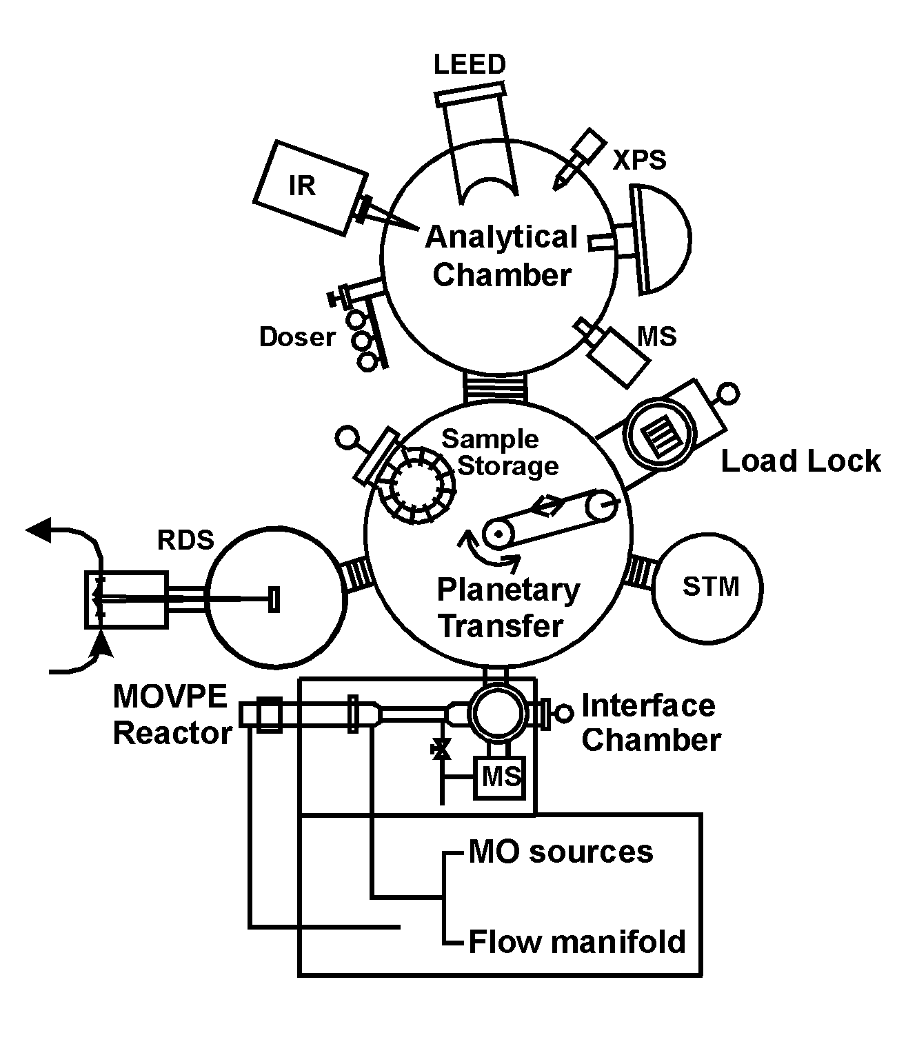
     In our laboratory, we have integrated a metalorganic chemical vapor deposition (MOCVD) reactor together with an ultrahigh vacuum system that contains a full suite of surface science instrumentation.  With this unique facility, we can follow the atomic-scale processes that occur on semiconductor surfaces during crystal growth.

     Shown below is a schematic of our experimental apparatus.

UHVSystem.gif (31950 bytes)

XPS: X-ray photoemission

spectroscopy

STM: scanning tunneling

microscopy

LEED:  low energy electron

diffraction

MS: mass spectroscopy

IR: infrared spectroscopy

RDS: reflectance difference

spectroscopy

MOCVD: metalorganic chemical vapor

deposition

MOVPE: metalorganic vapor-phase

epitaxy


bullet

Atmospheric Plasma

     Our laboratory contains a variety of plasma sources for processing materials at low temperatures and at pressures between 20 and 760 Torr.  Many of these sources have been donated by or developed in conjunction with Surfx Technologies, LLC.  In addition, we have a state-of-the-art facility for obtaining temporally and spatially resolved optical absorption and emission spectra of the reactive species in the plasma.  Most of our ex situ measurements are performed using the Nanolab cleanroom facility at UCLA.

     Presented in the figure below is a schematic of our apparatus for obtaining time-resolved UV absorption and optical emission measurements of the plasma afterglow.  This apparatus is explained in our upcoming paper by Jeong et al. in the Journal of Physical Chemistry (Publication 34).


     We have also developed a novel method for measuring the O-atom concentration produced by our plasmas using NO titration (Publication 109).  This method may be applied to other atomic species detection by selecting an appropriate titration gas with well documented chemical kinetics.
 
 
bullet

Computations

     We have recently built up our capabilities for computing the physical phenomena observed in the experiments.  In particular, our laboratory houses a Beowulf Linux cluster with 8 nodes (256 MB and 800 MHz each) for parallel computing, and two separate PCs for less demanding applications.  Installed on these computers is the Gaussian98 software suite for Ab Initio calculations of molecular clusters (up to 60 atoms).  With these clusters, we are simulating the atomic structure of compound semiconductor surfaces (see Publication 32).

     We have a dozen or so other PCs that are equipped with a variety of software for simulating the chemically reacting flows in MOCVD and plasma reactors.  For example, we have purchased FEMLAB and MATLAB software for simulating the gas and surface reactions that occur downstream of the discharge in our plasma-enhanced chemical vapor deposition (PECVD) reactors.


© Copyright 1996-2007, R. F. Hicks, Semiconductor Material Chemistry and Plasma Processing Laboratory, University of California, Los Angeles.

For information, please contact Professor Robert F. Hicks
Last Modified May 21, 2007 05:58 PM