Surfaces of InAs and InGaAs (001) in MOCVD
Surfaces of InAs and InGaAs (001) in MOCVD |
We have successfully grown epitaxial InAs and InGaAs films in our MOCVD reactor. Shown below are some of the STM images obtained. To learn more, please see our publications. |
|
|
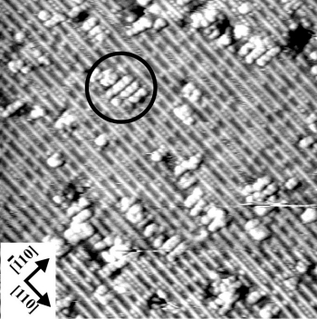
InAs (4x2) An InAs film of less than 10Å was deposited on a Ga-rich (4x2) gallium arsenide surface in the MOCVD reactor. Note the patches of arsenic-rich (2x4) found mixed in with the (4x2) phase (inside of the circle). This is due to the background arsenic pressure present in the reactor at 620ºC.
|
|
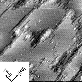
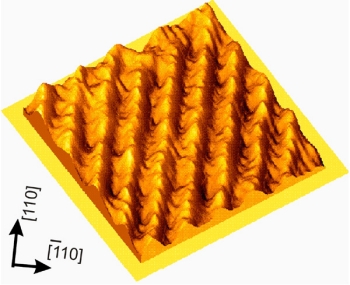
InGaAs (3x2) In0.05Ga0.95As films were deposited on GaAs (001) substrates in the MOCVD reactor at 550ºC. The sample was then annealed in UHV at 500 ºC to produce the (3x2) reconstruction shown on the left. The (3x2) consists of single rows of Ga dimers alternating between the first and third layers (refer to lower image). The surface does not follow the electron counting scheme seen for GaAs (001) reconstructions. |
|
© Copyright 1996-2007, R. F. Hicks, Semiconductor Material Chemistry and Plasma Processing Laboratory, University of California, Los Angeles. |
| For information, please contact Professor Robert F. Hicks |
| Last Modified May 21, 2007 05:58 PM |