Surface Reconstructions of InP (001)
Surface Reconstructions of InP (001) |
The surface structures of InP (001) are completely different from their counterpart on GaAs (001). Several STM images published in PRL and PRB are shown below. |
|
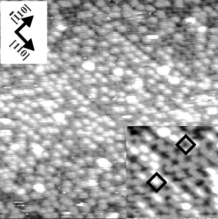
c(2x2)/p(2x2) The freshly MOCVD grown InP (001) thin film is covered with P ad-dimers, alkyl groups and hydrogen atoms. The phosphorous ad-dimers form a c(2x2)/p(2x2) structure on the surface.
|
|
|
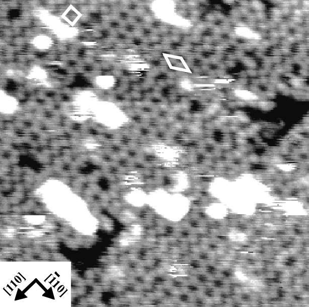
(2x1) Slightly annealing the c(2x2)/p(2x2) surface in vacuum at 300 oC results desorption of the P, CHx, and H adsorbates. The surface becomes (2x1), which is covered with a complete layer of P dimers. Electron counting reveals that there are only three dangling electrons associated with each dimer. The honeycomb structure highlighted in the image is a higher ordered c(4x2) reconstructions |
|
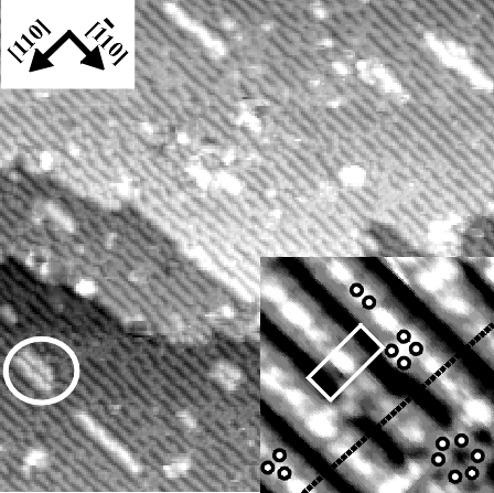
InP s-(2x4) Further annealing of (2x1) surface at 400 oC for 30 min leads to desorption of phosphorous from the surface. The surface becomes an indium-rich s-(2x4). For each (2x4) unit cell, there is one phosphorous dimer in the top layer and four indium dimer in the second layers |
|
|
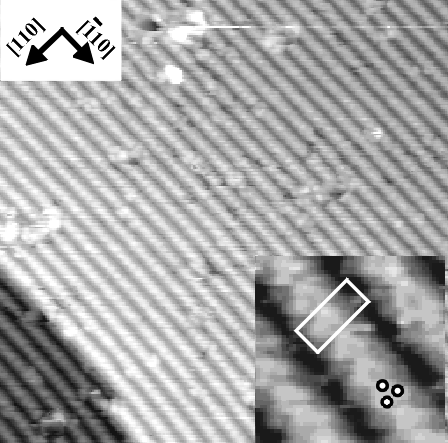
InP d-(2x4) s (2x4) surface can be further converted to d (2x4) by replacing the P-P dimer with a In-P mixing dimer. This surface shown on the left was obtained by annealing the InP crystal at 500 oC. The triangular spots highlighted in the image is corresponding to one P dangling bond and two In-In backbonds. |
© Copyright 1996-2007, R. F. Hicks, Semiconductor Material Chemistry and Plasma Processing Laboratory, University of California, Los Angeles. |
| For information, please contact Professor Robert F. Hicks |
| Last Modified May 21, 2007 05:58 PM |