Porous Si
![]()
![]()
![]()
![]()
|
Porous Si
|
|
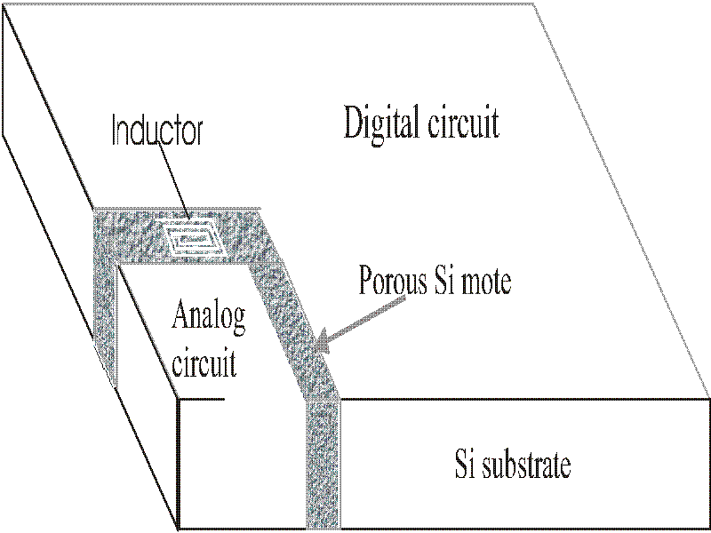
Cross-talk Isolation Using Porous Si for Mixed-signal Integrated Circuits Introduction
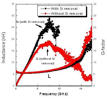
Portable electronics, especially the Si IC's for cellular telephone handsets, is the fastest growing sector of the entire microelectronics industry. Key components of today's cellular telephone handset consist of radio frequency (RF) power amplifiers, intermediate frequency (IF) mixers, and base-band circuitry that are typically in GaAs, Si bipolar, and Si CMOS technologies, respectively. Improvements on all key issues pertinent to portable electronics, namely, form factor, power consumption, and cost, will result if the various circuit components are integrated on a single Si chip. Such increased degree of integration is hampered by the cross-talk issue, for which there is no viable solution at current time. The cross-talk problem refers to the interference of digital and analog signals when they are integrated on the same Si chip. The switching of a digital circuitry with amplitudes on the order of volts sends wide spectrum noise that causes the potential at each point throughout the chip to fluctuate. The RF power amplifier is amplifying any input signal by a factor as large as 106. A mV fluctuation at the input end of the amplifier becomes noise of the order of volts at the output end, which renders the chip non-operational. Various measures have been used to minimize the problem, such as guard rings, multiple tube structures, SOI, differential input, and innovative circuit techniques. The typically achievable -60 dB of noise power from cross-talk interference is far from meeting the requirement of even today's cellular telephone handsets. Mixed signal circuits are the basis for many other applications, such as DSL modems that often require much lower cross-talk (~ -120 dB). New isolation technology is definitely needed in order to be prepared for the requirement of future generations of systems. Our research tackle the cross-talk problem by developing a Si VLSI compatible process module consisting of a high impedance porous Si mote around the RF power amplifier. The porous Si formation process converts Si with resisitivity as low as 0.005 ohm-cm in the bulk form to as high as 1010 ohm-cm in the porous form. This cross-talk isolation scheme should for the first time allow the integration of high performance digital circuitry and RF power amplifier on the same Si chip that will meet the stringent demand of markets, including cellular telephone hand sets and high speed modems. Moreover, it will enable the integration of high performance passive components such as spiral inductors and capacitors on the same Si chip. The ultimate goal of our research is to develop a Si VLSI compatible process module that will allow the incorporation of semi-insulating porous Si regions into Si chips. The objective is to offer a comprehensive solution to the challenges of mixed-signal integration technology that include cross-talk isolation, on-chip spiral inductor and precision capacitor. Porous Si material properties, VLSI processing compatibility issues, and the understanding of the dominant channels of substrate cross-talk interference are three key subjects that need to be addressed for achieving the ultimate goal. Consequently, our research encompasses characterization of porous Si materials, fabrication of isolation structures, and benchmark measurements of cross-talk isolation effectiveness using testing circuits. While it is relatively straightforward to understand the concept of using porous Si for RF isolation, many challenges remain in reducing the concept to a process module compatible with conventional VLSI technology. Regarding porous Si material, issues such as the long-term stability and the micro-structural dependence of the electrical conductivity, the implication of the small but non-zero internal stress, and the thermal stability, have to be addressed. The effectiveness of using porous Si region for high Q inductors has been demonstrated. The maximum Q of 20 obtained from the on-chip inductor at 2 GHz clearly shown the effectiveness of porous Si isolation. In this case, the porous Si region serves as a mechanical support for the inductor that separates the inductor from the underlying low resistivity Si substrate . The separation is on the order of several hundred microns, the penetration depth of the magnetic field. Consequently, the Eddy current loss and the capacitive coupling are greatly reduced, resulting in the high Q value and the high resonance frequency. |