Quantum Dot
![]()
![]()
![]()
![]()
|
Quantum Dot
|
|
fabricating organized quantum dot arrays by epitaxy Along with the continued shrinking of device dimensions in Si VLSI, the task of exploring and understanding new device structures that are based on quantum mechanical effects has become more urgent. These are devices with their critical dimensions smaller than the phase coherent mean free path of electrons, which is estimated to be on the order of 500 A in Si at room temperature. This need for novel device structures and technology is well recognized by the semiconductor industry which has called for the research and development of "novel device structures such as inherently self-aligned or adaptive transistors, or non-lithographically defined structures" . One such group of devices is based on semiconductor islands that are formed during hetero-epitaxial growths, also known as self-assembled quantum dots (SAQD). Island formation is driven by the compressive strain that is present in hetero-structures such as InAs on GaAs substrate and Ge on Si substrate. For electronic applications such as quantum computing, uniform size and spatial distribution is especially important as has been widely recognized by the research community in general. The separation between dots determines the tunneling probability or the wavefunction overlap that is analogous to the resistance of a conducting path. The variation in the quantum dot size could smear individual Eigen states of the dots and therefore the peaks and valleys in the I-V characteristics. Such requirement for optoelectronic applications, e.g. in quantum dot lasers, is much less stringent. Our main objective is to explore the limit in quantum dot size uniformity and spatial distribution regularity of the self-assembled system. Our research focuses on quantities that are intrinsic to the dot formation process such as the island nucleation process on a surface with periodic variation of lattice constants, and the existence of a limiting island size due to the strain accumulation at the core of a growing island/dot. With the understanding of the formation mechanism of SAQD’s, we will explore a variety of approaches to produce substrates with periodic variation of lattice parameters at the surface on the nanometer scale.
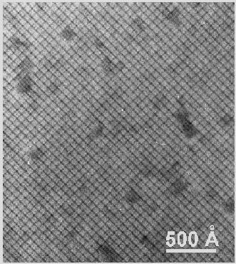
Figure 1 shows the transmission electron micrograph of one such substrates fabricated by Dr. Chih Chen.
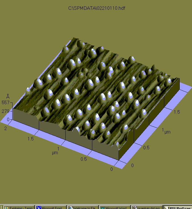
Figure 2 shows the atomic force micrograph (2 mm x 2 mm scan) of Ge islands grown on top of a patterned substrate. |