![]()
![]()
í@
|
Analysis of failure induced by temperature cycles in composite and eutectic SnPb flip chip solder joints (Unpublished report) K. N. Tu Dept. of Materials Science & Engineering, UCLA, Los Angeles, CA 90095-1591 í@ I. Introduction - Microstructure of flip chip solder joints The composite flip chip solder joint is defined to consist of a high-Pb solder (say 90Pb10Sn solder) on the Si chip side and a eutectic SnPb on the substrate side. The composition of the eutectic SnPb will be around 60Pb40Sn. The substrate is assumed to be BT resin. In the composite joint, the eutectic SnPb will be deposited or pasted on a Cu pad on BT to form solder-on-pad (SOP) before it is reflowed to join to the high-Pb. Figure 1(a) depicts the cross-section of a flip chip composite solder joint. We note that in the reflow, the eutectic SnPb will wet the high-Pb bump and form a coating around the high-Pb. We assume a layer of solder of thickness h' near the composition of eutectic SnPb remains. Figure 1(b) depicts the cross-section of a eutectic SnPb flip chip solder joint. The main difference between Fig. 1(a) and 1(b) is that the joint in Fig. 1(b) is a homogeneous eutectic solder joint. Here we have ignored different intermetallic compound formation in these two kinds of joints. To consider physical properties of the solders, for simplicity, we shall use pure Pb to represent the high-Pb. Actually the yield stress of 90Pb10Sn should be higher than that of pure Pb. We also include data of pure Sn for comparison. We find that,
It is important to note that the eutectic SnPb (the middle column) has the lowest yield stress, which means that when the applied stress in the composite solder joint is beyond the yield stress, the eutectic SnPb will deform first.
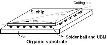
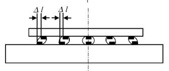
II. Thermal stress/strain induced by temperature cycling When the eutectic SnPb is reflowed to join the high-Pb, the reflow temperature will be slightly above the melting point of the eutectic, which is about 183 oC. Because the thermal expansion of Si and BT is different, it will induce a thermal stress in the packaging. We shall ignore it here, instead we shall concentrate on the thermal stress in temperature cycles between 20 oC and 105 oC. The latter is about the device operation temperature. So DT = 85 oC. The thermal expansion coefficient íža" of Si and BT are 2.6 ppm/oC and 25 ppm/oC, respective, so Da = 22.4 ppm/ oC. Thus the thermal or shear strain will be Now in Figure 2(a), we depict a schematic diagram of a flip chip. The largest shear strain will occur at the corner solder bumps at the diagonal direction of the Si chip. If we assume the size of the Si chip to be 1 cm x 1 cm, we have l = 21/2/2 cm = 0.707 cm, which is the distance of half of the diagonal of the chip, measuring from the center of the chip to its corner. Substituting the values of Da , DT, and l into Eq. (1), we obtain úGDl = 13.5 µm. We have ignored the tensile strain in the above analysis. In Figure 2(b), we depict the deformation of an array of solder joints by the thermal stress. It is known that the electronic industry has used underfill to redistribute the thermal stress. If the underfill has low glass transition temperature, it becomes soft at the device operation temperature, and the thermal stress will be taken up mostly by the solder joints. The solder joint at the corners will fail first.
III. Failure analysis To consider failure caused by the thermal stress, if we assume the height of the solder bump to be h = 100 µm, thus the shear strain is úGDl/h = 13.5/100 ~ 13 %. We recall that elastic limit is only 0.2 %. Then if we multiple it by the modulus (Let us assume the Young's modulus and the shear modulus are not that different) as given in the last section on Introduction, we shall have the stress, which is much greater than the yield stress. Thus, the joint will be deformed plastically. However, in the composite solder joint, when the layer of eutectic SnPb yields first, its thickness is much less than the total height of the solder bump. If we assume the thickness of the eutectic SnPb layer to be h' = 10 µm, the shear strain in it will be úGDl/h' = 13.5/10. Clearly the strain in the eutectic SnPb layer (in the composite solder joint) is about one order of magnitude higher than that in the homogeneous eutectic SnPb solder joint. Furthermore, strain energy is given as stress times strain and it will be proportional to the square of strain, so the strain energy imparted to the eutectic SnPb by the thermal stress will be about 100 times larger than that to the eutectic SnPb solder joint. If we define that due to temperature cycles, the failure occurs when the accumulated strain energy is beyond a certain threshold value, then fracture will occur and the joint will fail. We will not discuss the failure mechanism, e.g., how the crack nucleates and propagates, instead we just define the energetic criterion of failure as below. When the accumulated plastic energy is beyond a critical value of Wcrit, failure occurs.
where (DW/VDt) is the plastic strain energy produced per unit temperature cycle per unit volume of the solder, having a unit of joule/cm3-sec, V is the volume of the solder in units of cm3,Dt is the period of one temperature cycle, in units of sec. In each cycle, there will be elastic deformation as well as plastic deformation. We assume that when the total plastic energy or work-done to the solder is beyond a threshold value, it will crack due to excessive work hardening and sever plastic deformation. Since the plastic energy produced in the eutectic SnPb layer in the composite joint is about 100 times larger than that in the homogeneous eutectic SnPb joint, we expect the cycle times needs to fail the latter will be 100 times longer. But the above model is ideal, nevertheless it is reasonable to say that it is at the least 10 times longer. It is worth noting that the size of the chip can change and the thickness of the eutectic SnPb layer, h', in the composite can change, yet the overall outcome and reasoning remain the same.
IV. Other considerations (a) Stress relaxation In the above analysis, we have not considered stress relaxation. Since solder materials have a high homologous temperature at the device operation temperature, a certain amount of stress relaxation can occur, especially by creep. In creep, atomic diffusion is driven by a stress gradient. We shall consider the rate of diffusion in the solder joint first and then discuss the stress gradient. If we take lattice diffusivity in eutectic SnPb to be
where D0 is pre-exponential factor, which can be taken to be about 0.1 cm2/sec, úGH is activation enthalpy of diffusion, which for eutectic SnPb can be taken to be about 0.8 eV/atom, and kT has the usual meaning of thermal energy. At 105 oC, we obtain D ≈ 10 -12 cm2/sec. In a period of time of 12 hours, the diffusion distance can be estimated to be about 2 to 5 µm. At room temperature, the diffusion distance will be much smaller. For creep to reduce stress, the atoms may need to diffuse to the free surface of the solder joint (because of stress gradient), which has an average distance of half of the diameter or half of the height of the solder bump, which is about 50 µm. Thus creep will not be able to relax all the stress and strain. If atoms diffuse instead to internal surfaces, grain boundaries, or dislocations, it tends to cause void formation and crack formation and enhances failure. (b) Electromigration While the high-Pb solder is known to have better resistance to electromigration, eutectic solder is not, especially when current crowding occurs at the cathode entrance where the electrons enter the solder bumps. When the applied current density is above 5 x 10³ A/cm2, electromigration occurs rather faster in the eutectic solder. Whether electromigration will enhance the failure caused by temperature cycle or power cycle is unclear at the moment. It needs to be addressed. (c) Intermetallic compound formation The distribution of intermetallic compound (IMC) in the flip chip solder joint should be investigated to see if it has any effect on the fracture failure. A very thick IMC will enhance the model of failure presented in the above. (d) Coffin-Manson model of low cycle fatigue failure The classic model of low cycle fatigue failure in high-Pb C-4 solder joints (not the composite solder joint) has been investigated by the model of Coffin-Manson in which a power relation between plastic strain and number of cycle was given. It will not be reviewed here. But it will be of interest to see if the model can be applied to the failure observed in the composite solder joints under a very large strain.
V. Executive Summary The composite solder joint has a built-in weakness due to the thin layer of eutectic SnPb solder in the joint. The eutectic SnPb has a low yield stress and it will deform first and lead to stress concentration and to accumulate high plastic strain energy. The homogeneous eutectic SnPb solder joint tends to have a uniform composition and much lower plastic deformation so the accumulation of plastic strain energy per unit volume is lower. If we define the failure by an energy criterion, the eutectic SnPb solder joint may have at least ten times longer life-time than the composite solder joint. For life-time prediction, the real microstructure of these two kinds of flip chip solder joint should be studied and actual failure rate should be measured. í@ Reference: K. N. Tu, ížSolder joint technology: Materials, properties, and reliability," Springer, New York (2007). í@ 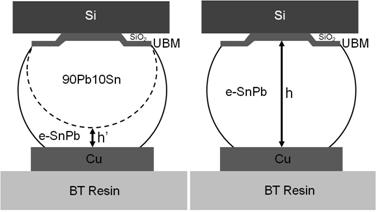 Fig. 1(a) Schematic diagram of the cross-section of a composite high-Pb and eutectic SnPbflip chip solder joint. (b) A eutectic SnPb flip chip solder joint. í@
Fig. 2(a) Schematic diagram of a flip chip on a substrate. The diagonal of the chip is shown.
Figure 2(b) Schematic diagram of the cross-section of an array of deformed solder joints under thermal stress.
|
||||||||||||||||
| í@ |