Recent Publications
GaAs nanopillars-array solar cells employing in situ surface passivation
GaSb/InGaAs quantum dot-well hybrid structures as active regions in solar cells
Strong passivation effect on the properties of InAs surface quantum dot hybrid structure
Enhanced InAs nanopillar electrical transport by in-situ passivation
800 meV localization energy in GaSb/GaAs/Al0.3Ga0.7As quantum dots
Effects of GaAs(Sb) cladding layers on InAs/AlAsSb quantum dots
Strongly coupled slow-light polaritons in disordered one-dimensional localized states
Tuning quantum dot luminescence below the bulk band-gap using tensile strain
News
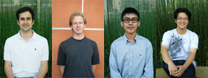
(L-R) Charles Reyner, Joshua Shapiro, Chester Hung, Clayton Tu
Congratulations to the graduating members of INML
Charles Reyner graduated with a Ph.D. and will be working in the Sensors Directorate of the Air Force Research Lab (AFRL) at Wright-Patterson Air Force Base (WPAFB) in Dayton, Ohio. His position focuses on the growth of novel III/V heterostructures using molecular beam epitaxy. Charles was an ASEE SMART Fellowship recipient from Fall 2011 through graduation in June 2013. The SMART Fellowship provided both his stipend and tuition, while giving an opportunity to intern at WPAFB during Summer 2012.
Joshua Shapiro graduated with a Ph.D. and will be working at Northrup Grumann in their management training program in the area of cyber security. Joshua was a NSF-IGERT Clean Energy for Green Industry (CGI) trainee from Fall 2009 through graduation in June 2013. The CGI Traineeship provided both his stipend and tuition in alternate years, giving an opportunity to attend the DFT and Beyond Workshop in Berlin, Germany.
Chester Hung graduated with a Master's and will be working at Nanopixel, a spin-off company spearheaded by graduate student Pradeep Senanayake. Chester's research was on plasmonic nanopillar photodetectors, modeling the optical and electrical characteristics of the device structure.
Clayton Tu graduated and will be working at HRL Laboratories. Clayton worked with growth and device characterizations, including photoluminescence (PL) measurements as well as current/voltage (IV) measurements.
![]()
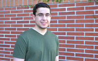
(L-R) Alan Farrell, Chester Hung, Prof. Diana Huffaker, Pradeep Senanayake
Nanopixel Technology: A New Spin-Off Company
A new spin-off company has been formed based on UCLA-owned IP out of the INML lab. Nanopixel Technology is SBIR (Small Business Innovation Research) funded and focuses on nanopillar/plasmonic based photodetector technology. The goal is to commercialize nanopillar based plasmonically enhanced detectors for high sensitivity high bandwidth receiver applications. Pictured to the right are Prof. Diana Huffaker and the graduate students who have formed Nanopixel Technology, Alan Farrell, Chester Hung, and Pradeep Senanayake (left to right).
Patents Filed
Charles Reyner has filed for "Avalance Photodiode Utilizing an Interfacial Misfit Array".
Michael Haddad Awarded NSF Graduate Research Fellowship
Michael Haddad has been awarded the prestigious NSF Graduate Research Fellowship, providing full support for three years. The fellowship recognizes and supports outstanding graduate students in NSF-supported science, technology, engineering, and mathematics disciplines who are pursuing research-based masters and doctoral degrees at accredited U.S. institutions. Michael's research focuses on growth, device fabrication, and characterizaton of III-V semiconductor nanostructures. Previously, Michael had been awarded the NSF-IGERT Clean Energy for Green Industry at UCLA traineeship.

Alan Farrell Awarded UCOP Cote-Robles Fellowship
Alan Farrell has been awarded the Eugene V. Cote-Robles Fellowship. It is a four-year fellowship program funded by the University of California Office of the President with the aim of providing access to higher education for students from underrepresented groups. Alan's research is on nanopillar-based avalanche photodetectors for near- and mid-wave infra-red radiation. He hopes to reduce, or eliminate, the need for costly cooling systems required by current state-of-the-art detectors, thereby reducing the weight and power consumption of these devices. Previously, Alan had been awarded the NSF-IGERT Clean Energy for Green Industry at UCLA traineeship.
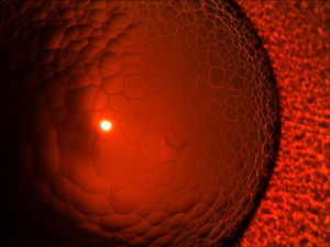
Dr. Paul Simmonds Wins Image of Distinction Award at Nikon Small World 2012 Photomicrogaphy Competition
Subject matter: A semiconductor sample thinned down to electron transparency using an argon plasma (50x)
Technique: Brightfield
The Nikon International Small World Competition first began in 1975 as a means to recognize and applaud the efforts of those involved with photography through the light microscope. Since then, Small World has become a leading showcase for photomicrographers from the widest array of scientific disciplines.
The Nikon Small World Competition is open to anyone with an interest in photography through the microscope. Truly international in scope, entries have been received from the United States, Canada, Europe, Australia, Latin America, Asia, and Africa. Winners have included both professionals and hobbyists.
Entries submitted to Nikon are then judged by an independent panel of experts who are recognized authorities in the area of photomicrography and photography. These entries are judged on the basis of originality, informational content, technical proficiency and visual impact.
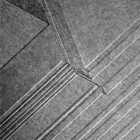
Andrew Lin Wins Third Place for the FEI Company Tony Award For EICN TEM Imaging Contest 2012
Title: Chainmail Defects in a GaAs nanopillar grown on Si
Description: This is a 200 nm X 200 nm bright-field TEM image of a GaAs nanopillar cross-section. The nanopillar was grown by selective-area epitaxy using metal-organic chemical vapor deposition on a Si (111) substrate. The image was taken using a FEI Titan at 300 kV with a zone axis of [110]. High quality III-V semiconductors grown on Si have the potential for CMOS-compatible optoelectronic and electronic devices. Nanopillars have been shown to achieve such high quality growth on Si. However, if the growth conditions are slightly off, these types of crystal defects can form in the core of nanopillar creating grain boundaries with different atomic orientations. The image was taken with the FEI Titan S/TEM microscope.
Joshua Shapiro Wins Best Student Presentation At EMC
In the 2011 Electronic Materials Conference in UC Santa Barbara, graduate student Joshua Shapiro presented a paper entitled, "Structural Characterization of InGaAs Axial Inserts in GaAs Catalyst-Free Nanopillars Grown by Selective-Area MOCVD", co-authored by Andrew Lin and Professor Diana Huffaker. Joshua Shapiro's entry was selected as one of two Best Student Presentations by the committee.
Joshua presented a study of axial GaAs/InGaAs hetro-interface formation in catalyst-free nanopillars grown by selective-area MOCVD. The focus was on controlled growth of axial heterostructures as capability key for enabling efficient nanopillar light emitters and detectors, and preliminary light-emitting devices with axial double heterostructures grown on silicon.
The award, accompanied with a monetary prize, will be presented at the 2012 EMC Meeting in Penn State University on June 20, 2012. The EMC is a premier annual forum for the preparation and characterization of electronic materials sponsored by The Minerals, Metal and Materials Society Foundation.
About the Lab
The Integrated NanoMaterials Core Lab (Prof. Diana L. Huffaker Research Group, Electrical Engineering Dept, California NanoSystems Institute, UCLA) is devoted in conducting research on topics on optoelectronic devices enabled by atomic self-assembly at the heterointerface in novel compound III-(As, P, N Sb) materials for Si photonics, single photon sources, MWIR applications and solar cells. Unique aspects of our research include nanoscale-confined epitaxial processes in patterned and self-assembled quantum dots and device integration enabled by interfacial misfit arrays.