Members
Graduate Students | Undergraduate Students | Postdoctoral Scholars | Research Staff | Past Members
Dr. Diana L. Huffaker
Professor, Electrical Engineering Department
Director, Integrated NanoMaterials Core Lab, California NanoSystems Institute
Director and PI, NSF-IGERT Clean Energy for Green Industry at UCLA
Education:
PhD, Material Sciences, University of Texas, Austin
MS, Material Sciences, University of Texas, Austin
BS, Engineering Physics, University of Arizona
Biography:
Prior to teaching at UCLA, Professor Diana Huffaker was a faculty member in the Department of Electrical and Computer Engineering at the University of New Mexico, Albuquerque. Her research interests cover nanodot-based optoelectronic devices including III-V/Si photonics, lasers, single-photon emitters, III-V nanotransistors, solar cells and electronic characterization of biomaterials. Her current research projects focus on device development, crystal growth (MBE and MOCVD) and characterization of patterned and self-assembled quantum dots in compound III-(As, P, N, Sb), modeling of self-assembled processes along with electronic characterization of biomaterials.
Research Interests:
Directed and self-assembled nanostructure solid-state epitaxy, optoelectronic devices including solar cells and III-V/Si photonics.
Awards:
2010 SPIE, Nanotechnology Innovation Award
2008 DoD, National Security Science and Engineering Faculty Fellow (NSSEFF)
2008 IEEE, Fellow
Graduate Students

Ting-Yuan Chang, Ph.D. course
Email: tychang1014n@ucla.edu
Research Interests:
Metal-organic chemical vapor deposition (MOCVD) growth
Selective areaepitaxy of III-V nanopillar-based devices on SOI platform
Nanofabrication
Zixuan Rong, Master course
Email: rongzixuan789@ucla.edu
Research Interests:
3-D nanowire modeling
III-V nanowire growth by epitaxy
THz emitters
Andrew Chen, Master course
Email: andrewclair05231210@gmail.com
Research Interests:
III-V semiconductor photodetectors and photovoltaics
III-Sb APDs and photon counting detectors for X-rays and gamma-rays
Postdoctoral Scholars
Research Staff
Dr. Baolai Liang, staff research associate
Research:
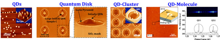
Semiconductor quantum dot (QD) nanostructures are the subject of increasing interest based on their potential for next generation of optoelectronic devices. However, due to the self-assembly process of forming QDs, the random distribution in size and position has degraded the performance of QD devices. Therefore, control of the size, shape, density and position of QDs has become an important research task.
Research Interests:
Fabrication and characterization of the ultra-high density (>1011QDs/cm2), ultra-low density (<108QDs/cm2), and laterally-organized semiconductor QDs via both "top-down" and "bottom-up" methods, especially by selective area growth and droplet epitaxy technique. These QDs are useful for versatile devices like laser, detector, solar cell, modulator, quantum gate, single photon source, etc.
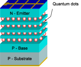
Dr. Ramesh B. Laghumavarapu, staff research associate
Biography:
Dr. Laghumavarapu received his B.Sc, M.Sc and M.S degrees from Nagarjuna University, University of Hyderabad and University of Massachusetts Boston in 1997, 2000 and 2003 respectively. He graduated with his Ph. D. degree from University of New Mexico in 2008. He worked as a Senior Scientist at Quanlight Inc; before joining Electrical Engineering, University of California Los Angeles as a Post Doctoral Researcher.
Research Interests:
Quantum dot solar cells, III-Sb based thermophotovoltaics on GaAs substrates and nanostructure based hybrid solar cells.
Visiting Scholars
Undergraduate Students
Minh Cao
Research Interests:
Siddharth Somasundaram
Research Interests:
Past Members
Dr. Bor-Chau Juang
Research Interests:
III-V semiconductor photodetectors and photovoltaics
III-Sb APDs and photon counting detectors for X-rays and gamma-rays
III-Sb optoelectronic devices grown on highly mismatched GaAs using IMF arrays
Dr. Dingkun Ren
Email: dingkun.ren@ucla.edu
Research Interests:
Nanomaterials, nanophotonics/nanoplasmonics, nanowires, MOCVD
InAs(P)(Sb) nanowire-based optical devices: photodetectors at short-wave infrared (SWIR) and mid-wave infrared (MWIR), quantum-well infrared photodetectors at long-wave infrared (LWIR), THz quantum cascade lasers (QCLs)
Selective-area quantum-dots (QDs) in nanowires
3-D nanowire modeling
Dr. Hyunseok Kim
Email: hyunseokkim [at] ucla [dot] edu
Research Interests:
III-V nanowire optical links
- Nanowire bottom-up photonic crystal lasers on Si photonic platforms
- Photonic-plasmonic hybrid nanowire photodetectors
Alan Farrell, graduate student
Fellowships:
NSF-IGERT: Clean Energy for Green Industry at UCLA
Research Interests:
New light trapping techniques using photonic crystals, renewable energy, photovoltaics, nanopillar arrays.
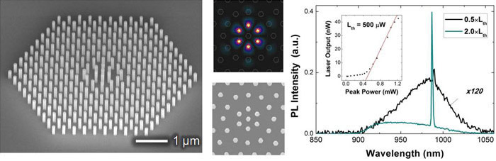
Dr. Wook-Jae Lee, postdoctoral scholar
Research Projects:
High quantum efficiency MidIR nanopillar photodiodes
Nanopillar array lasers
Nanopillar-based energy efficient optical links on SOI
Dr. Adam Scofield, postdoctoral scholar
Research:
Adam's research is focused on the design, growth, and fabrication of bottom-up photonic crystal devices on silicon. By using MOCVD grown catalyst-free III-V nanopillars, both photonic band-gap regions and active regions can be grown simultaneously on a Si(111) substrate. This approach to photonic crystal lasers has several advantages that are unique to the catalyst-free growth technique:
- Axial InGaAs inserts in the GaAs nanopillars can be extended to longer wavelengths such as 1.31 and 1.55µm in the active regions
- The diameter dependence on the vertical growth rate results in a blue shift in the absorption peak of the pillars in the photonic band-gap region preventing reabsorption losses.
- The crystallographic surfaces will minimize loss from the cavity mode due to surface roughness.
- In-situ passivation by growth of InGaP shells is used to prevent non-radiative surface recombination that is detrimental to device performance.
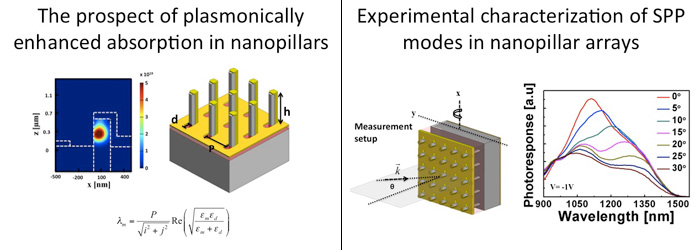
Dr. Pradeep Senanayake, postdoctoral scholar
Research project:
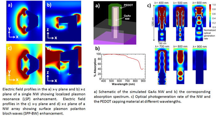
Nanopillar-based plasmonically enhanced photodiodes (NP-PEPDs)
- Nanopillar-based plasmonically enhanced photodiodes (NP-PEPDs) have several advantages over conventional planar photodiode technology in terms of reduced leakage current from the small footprint of nanopillar arrays and enhanced collection efficiency from the effective "plasmonic antenna" from the self aligned subwavelength metal holes.
- The "plasmonic antenna" effectively collects light from a large area and concentrates it on a much smaller nanopillar junction reducing the junction capacitance and transit time of photocarriers.
- Plasmonic resonances consist of both propagating surface plasmon polariton modes and localized surface plasmons due to the shape resonance of the subwavelength metal hole.
- In principle, this allows the reduction of the detector volume even below the diffraction limit for more efficient integration and reduced material growth requirements, reduction of the leakage current for greater detector sensitivity, and reduction of the junction capacitance and transit time for higher speed detectors.
Dr. Giacomo Mariani, postdoctoral scholar
Research:
Mariani's research is currently focused on several types of nanostructured solar cells: hybrid nanopillar solar cells that take advantage of both organic chemistry (semiconducting polymers) as well as inorganic chemistry (III-V semiconductor nanowires), all-epitaxial III-V nanopillar solar cells and recently II-VI colloidal quantum dots on III-V nanopillar solar cells. His goal is to demonstrate efficient nanostructured photovoltaic devices.
Dr. Paul Simmonds, staff research associate
Biography:
Paul received his Ph.D. in Semiconductor Physics from the University of Cambridge in 2008. He worked as a Postdoctoral Associate, first with Prof. Chris Palmstrøm at UCSB, and then at Yale University with Prof. Minjoo Larry Lee. He joined CNSI-UCLA as manager of the Integrated NanoMaterials Laboratory in September 2011.
Research Interests:
Molecular beam epitaxy (MBE) provides the foundation for much of Dr. Simmonds' research. MBE is an incredibly versatile tool that allows the user to create exceptionally pure thin-films from a wide range of different elemental ingredients. He is interested in novel approaches to synthesizing technologically important nanostructures and materials: from self-assembled quantum dots, to large-area sheets of graphene.
The recent installation of a new III-N MBE chamber provides the INML with the ability to combine technologically important nitride materials with well-established device architectures based on Si or GaAs (for example). Paul is investigating approaches by which to integrate nitride films and nanostructures with dissimilar semiconductor platforms, and in doing so to access exciting new functionalities.
Meng Sun, graduate student
Research:
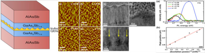
My current project is the development of intermediate band solar cells (IBSCs) based on the use of quantum dots (QDs). Our work centers on InAs QDs surrounded by AlAsSb barriers lattice matched to InP. InAs self-assembles into 3D nanostructures when deposited onto AlAsSb lattice-matched to InP. However, when we embed InAs QDs directly within AlAsSb barriers we find a poor photoluminescence (PL) response, so we introduce thin cladding layers of GaAs1-xSbx above and below the InAs QDs to improve their quality. By using these GGaAs1-xSbx cladding layers to effectively reduce the presence of Sb adjacent to the InAs, improved morphology and optical response are achieved. The power-dependent PL of these QDs confirms that we have type-II band-alignment, which is beneficial for IBSCs application due to the longer carrier life time.
Andrew Lin, graduate student
Research Interests:
Study of structure, spectral and transport characteristics, and the effect of surface states of III-V semiconductor nanopillars grown by MOCVD.
Chester Hung, junior development engineer
Research:
I am currently working on plasmonic nanopillar photodetectors. My main responsibility is to model the optical and electrical characteristics of the device structure. By using the FDTD solution program called Lumerical, I have produced results such as spectral responses and the effect of polarization of incident fields on the photodetector.
Michael Haddad, graduate student
Fellowships:
NSF-IGERT: Clean Energy for Green Industry at UCLA
Research Interests:
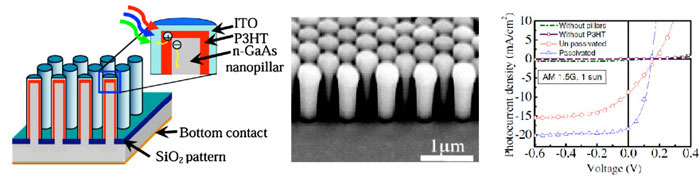
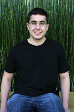
MOCVD grown catalyst-free selective-area III-V nanopillars used for both hybrid and all-epitaxial solar cells. Example of a hybrid solar cell is the PBnDT-FTAZ/GaAs heterojunction is pictured below. Also shown are two single layer graphene sheets acting as a transparent top contact to GaAs nanopillars. Additionally, Michael is attempting to grow catalyst-free InP nanopillars on inexpensive Silicon substrates.
Charles Reyner, graduate student
Research:
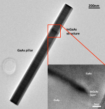
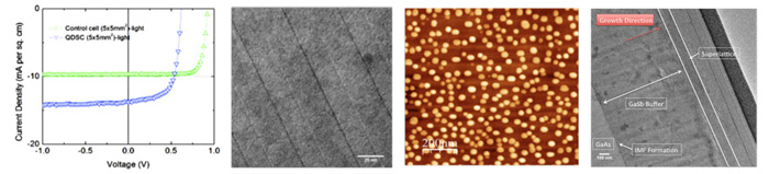
I am currently working on several projects, including quantum dot memory, quantum dot solar cells, infrared detectors on GaAs substrates, and defect-free III-Sb growth on silicon. The quantum dot (QD) work focuses on Type II GaSb/GaAs QDs. These QDs are of particular interest because of their long radiative lifetime. The long lifetime can be used to either store carriers in the QD (QD memory) or minimize carrier loss due to recombination (high-efficiency solar cells). Images below depict the high density (5.4 x 10¹⁰ QDs per cm2) of QDs, QDs in a solar cell, and the current-voltage performance of a QD solar cell versus a normal GaAs control cell under AM1.5 illumination. I am also developing InAs/GaSb superlattices on an interfacial misfit (IMF) array for use as infrared detectors. Typically, these structures are grown on GaSb substrates, which cost four times more than GaAs and have higher defect densities. However, by growing on IMF, I hope to improve the noise performance of these superlattice devices and bring down their cost. A TEM of a superlattice on IMF is pictured below.
Joshua Shapiro, graduate student
Fellowships:
NSF-IGERT: Clean Energy for Green Industry at UCLA
Research Interests:
Growth and characterization of high quality three dimensional heterostructures for optoelectronic devices.
Clayton Tu, research staff associate
Research:
I joined the group as an undergrad fellowship member in 2010. My main role is assisting the grad and post-doc students with growth and device characterizations. This includes photoluminescence (PL) measurements as well as current/voltage (IV) measurements. With two PL setups in the lab, one general and one micro, I help the group by taking room temperature, cold temperature (77K), power dependent, and temperature dependent PL measurements on quantum dots and nano-pillars. With a probe station setup, I also work with the group and do IV measurements on solar cell devices. I hope to gain experience on other characterization methods in the future.
Rockwell Arthur, lab assistant
About:
Rockwell Arthur attends Brophy College Preparatory where he is on the football team. He also DJs.
Chandler Hall, lab assistant
About:
Chandler Hall attends Brophy College Preparatory and is employed at Coffee Roasters of AZ. He has a black belt in tae-kwon-do, writes for his school's music magazine, and plays guitar.
Xu "Bird" Du, visiting undergraduate student
Fellowships:
Cross-disciplinary Scholars in Science and Technology (CSST)
Research:
Xu is a undergraduate student from Zhejiang University and is conducting research with the Huffaker research group under the program of the Cross-disciplinary Scholars in Science and Technology. Xu conducted research on the photoluminescence and photoluminescence excitation spectroscopy of intermediate-band solar cells with quantum dots. The application of plasmonic in solar cell and the simulation of different structures by FDTD Lumerical and COMSOL is also the interest of Xu.
Dr. Tugba Selcen Navruz, visiting scholar
Research:
Mathematical modeling and simulation of quantum-dot, quantum-well and tandem solar cells using Sentaurus TCAD. Optimization of solar cell structure for various materials to achieve maximum efficiency. The current project aims to optimize AlAs(Sb)/InAs(Sb) QD solar cell.
Jiri Thoma, visiting graduate student
Research:
Jiri Thoma was born in the Czech Republic in 1983. He received his M.Eng. degree in Radioengineering with specialization on optical fibre systems from Czech Technical University in Prague in 2008. In 2008 he joined Photonics Device Dynamics Group of the Tyndall National Institute led by Dr. Huyet as a Ph.D. student. His project studies the single-chip monolithic integration of laser with electro-absorption modulator on novel material system. In October 2011 he visited Prof. Huffaker group at UCLA for 2 months in direct collaboration with Dr. Liang on his project. He is also interested in the spread of mutual groups collaboration on Type-II GaSb QD mode-locked lasers.
Alissa Wiengarten, visiting graduate student
Research:
Alissa is working on her master's thesis in the group of Prof. Bimberg at TU Berlin. For a couple of months she joins the group of Prof. Huffaker to improve the collaboration between the two groups. The project she is working on is concerned with a quantum-dot-based memory device. The goal is to create a non-volatile memory device which consists of different semiconductor materials. Alissa works on the charactarization and improvement of a MBE-grown GaSb-quantum-dot material structure. The main characterization techniques are DLTS (Deep level transient spectroscopy), C(V)-measurements, Photoluminescence and Electroluminescence.
Dr. Andrew Marshall, visiting scholar
Research:
Dr. Marshall's research focusses on novel infrared photodetectors. He previously developed the first InAs avalanche photodiodes, demonstrating unique low noise and high bandwidth properties. He has also researched and fabricated travelling wave photodetectors for optical communications and avalanche photodiode arrays for LIDAR applications. He recently won a Royal Academy of Engineering research fellowship and is based at Lancaster University in the UK. During this fellowship he aims to engineer novel infrared photodiodes by exploit the interface misfit epitaxy technique, in collaboration with Professor Huffaker, improving performance and reduced cost.
Dr. Kalyan Nunna, staff research associate
Research Interests:
- Molecular beam epitaxial growth optimization of Antimonide-based materials monolithically grown on GaAs or Si substrates
- Develop group III-Sb based quantum wells and quantum dots for near and mid infrared light emitters.
- Design and develop long wavelength bulk photo detectors lattice matched to GaSb.
Zhuozhi "George" Yao, visiting undergraduate student
Fellowships:
Cross-disciplinary Scholars in Science and Technology (CSST)
Research:
George is a student at Peking University and is conducting research with the Huffaker research group through the Cross-disciplinary Scholars in Science and Technology (CSST) program. George conducted research on the optimization of III-V nanopillars for high efficiency solar cells.
Dr. Anitha Jallipalli, postdoctoral scholar
Research:
Dr. Jallipalli is involved with design, modeling, fabrication and characterization of interfacial misfit dislocation (IMF) array based p-n diodes for defect analysis. She is also working with the correspondence between reverse bias leakage and threading dislocation density. Her interests also include design, modeling, fabrication and characterization of III-Sb long wavelength monolithic, "buffer-free" edge emitting lasers, VCSELs and bulk GaInAsSb detectors deposited on GaAs, Si substrates.
Dr. Jun Tatebayashi, postdoctoral scholar
Research Project: Monolithic Active Silicon Nano-Photonics
Dr. Ping-Show Wong, postdoctoral scholar
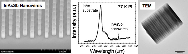
Research Project: Catalyst-Free Growth and Characterization of III-AsSb Nanowires by MOCVD
Nanowires provide a bottom-up approach for semiconductor fabrication to serve as building blocks for nano-sized structures and devices with designed dimensions and properties at desired locations. Among III-V semiconductors, antimony compounds are attractive for mid-infrared and electronic applications due to their small bandgaps and high carrier mobilities. In this study, we focus on the synthesis of GaAsSb and InAsSb nanowires on nanopatterned substrates by metal-organic chemical vapor deposition (MOCVD) in the catalyst-free growth mode. The material, optical, and electrical properties of these nanowires are characterized and analyzed.
Alexander Williams, graduate student
Fellowships:
NSF-IGERT: Clean Energy for Green Industry at UCLA
Biography:
Williams holds undergraduate degrees in Physics and Mechanical Engineering, with masters in ME from Columbia University. Currently in the Materials Science department.
Research Interests:
Epitaxially grown solar cells and thermoelectric devices using novel nanostructures such as quantum dots.
Devinna Fleming, undergraduate student
Fellowships:
NSF-REU: Integrated Optics for Undergraduates
Research Project:
My research is supported by a NSF Integrated Optics for Undergraduates (IOU) Research Experience for Undergraduates (REU) grant. This 9 week program includes a poster symposium, a presentation and a final paper on the research performed. My work focuses on increasing the density and quality of InAs quantum dots by incorporating Antimony surfactant layer to trigger the InAs QD formation. I am assisting with QD characterization (AFM, photoluminescence testing and data analysis). This work will benefit optoelectronic devices like QD lasers, detectors, solar cells and modulators.
Richard Gaona, undergraduate student
Research Project:
I am working with UCLA's Center for Excellence in Engineering and Diversity (CEED) through their Research Intensive Series in Engineering for Underrepresented Populations (RISE-UP) program, funded by a Lockheed Martin grant. Dr. Ramesh Laghumavarapu has been teaching me with two levels of Quantum Dot Solar Cell development: I-V characterization and device simulation using the PC application PC1D. Furthermore, I have benefitted from the wealth of information offered by my labmates and Prof. Huffaker in the areas of QDSCs and semiconductor physics.
Isaac Nacita, undergraduate student
Abhejit Rajagopal
Research Interests:
optical nanopillar solar cells simulation

Gabrielle Robertson
Research Interests:
Nicholas Benzoni
Research Projects:
LabVIEW programming
design, growth, and fabrication of bottom-up photonic crystal devices on silicon