|
|
| |
|
|
|
| |
|
|
 |
| |
|
|
|
Sean Wang,
PhD 2025, Lecturer, UCLA |
 |
|
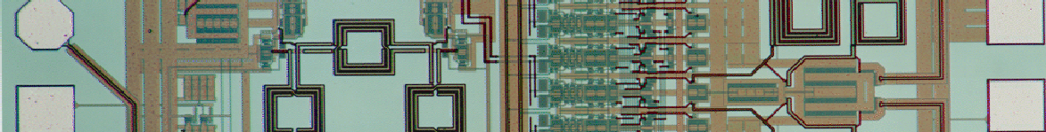
A 28-GHz 7.3-mW/Element Beamforming Receiver with On-Chip Local Oscillator (LO) Synthesis
 Utilization of the millimeter-wave (mmWave) frequency range for mobile applications was first introduced by 5G New Radio (5G NR) and is expected to remain a staple in future wireless systems, such as 6G and beyond. We focus our attention on frequency range~2 (FR2), which contains the mmWave frequency bands spanning from 24 to 44GHz, and with channel bandwidths of up to 400 MHz. The use of beamforming gives these radios a significant advantage for a longer range, but such a scenario becomes attractive only if the total power consumption and cost fall below those of Wi-Fi.
Research on beamforming receivers (RXs) has extensively targeted the N257/N258/N261 bands in the vicinity of 28 GHz for realization in CMOS technology. Per-element power draws of between 20 mW to 50 mW are reported. However, a key observation is that the local oscillator (LO) synthesis is either off-chip or on-chip via a centralized frequency synthesizer, necessitating extra power and area expenditure on LO routing and distribution circuitry. Furthermore, the phase shift networks required for beamforming typically consumes substantial power, whether they appear in the receive path or the LO paths.
This work introduces a new phase shifting method and stacking technique that are combined to realize a low power beamforming receiver that achieves high phase shift resolution with virtually no overhead. Several other new architecture and circuit techniques are also proposed to further reduce power consumption and improve area efficiency, resulting in the smallest area and lowest power reported to date. Realized in 28-nm CMOS technology, the eight-element RX occupies a total area of 2.01 mm2 and draws 7.3 mW per element. Each element achieves a minimum noise figure of 4.8 dB, a phase resolution of 10 degrees, and an uncorrelated LO rms jitter of 640 fs.
|
|
|
|
|
|
|
|
Chandrakanth Choppa,
PhD 2025, Engineer, Apple |
 |
|
New Frequency Synthesis Methods for the Millimeter-Wave Band
Congestion of radios at gigahertz frequencies is pushing communications into higher parts of the spectrum. The 140-GHz band presents an attractive medium for high-throughput wireless communications. A great deal of work has been expended on 6G radios for this band, but no fractional-N synthesizer operating at these frequencies has been reported. The
first part of the dissertation addresses this need. A single loop synthesizer architecture faces
rigid trade-offs among reference phase noise (PN), VCO PN and ΔΣ quantization noise
(Q-noise) making cascaded PLLs more desirable. However, the trade-off between the latter
two persists unless the ΔΣ modulator can be clocked at very high frequency. This is the
principal distinction between our approach and the prior art. Several novel circuit techniques
have been introduced to enable our proposed architecture, achieving a fourfold reduction in
jitter and a twofold reduction in power, compared to the state of the art. Fabricated in
28-nm CMOS technology, the PLL exhibits an rms jitter of 158 fs, consumes 26 mW while
occupying an area of 0.17 mm2, thus making it attractive for beamforming systems with one dedicated synthesizer per element.
Secondly, sampling phase detector (SPD) based PLL architectures are extensively researched and reported. The high gain of the SPD allows for significant in-band noise sup-
pression. Both the sampling PLL and the sub-sampling PLL architectures use this PD. In both, the PD noise and the charge pump noise is not multiplied by N2, irrespective of the presence or absence of the divider. Working of both these PLLs is presented to aid simpler
understanding and provide insights. A comparative study between these two PLLs is done,
highlighting the similar properties and differences.
|
|
|
|
|
|
|
|
Makar Chand Snai,
PhD 2024, Engineer, Apple |
 |
|
A 140-GHz 40-mW Receiver with LO(Local Oscillator) Signal Generation and Phase Shifting for Beamforming Applications
While the 5G standard has mainly focused on enhanced data connectivity, the next generation, 6G, will attempt to converge many technologies (AI, ML, communication, computing). The use of the D-band for its wide bandwidth is attractive for such systems. But the high path loss requires a large beam-forming array and hence high power consumption. Thus, compact, low-power D-band radios are of high interest. We describe a receiver with a minimum NF of 4.7 dB that draws 40 mW, a factor of 2.5 less than state of the art, and, requires only a 250-MHz reference frequency while providing a phase shift range of more than 180°in each beamforming element. This performance is achieved by several new techniques: (1) an RF path with low-impedance interfaces to ease the noise-stability trade-off, (2) a 94-GHz subsampling PLL, (3) a new quadrature LC QVCO, and (4) a new phase shift technique that resides at low frequencies. The new QVCO reduces the phase noise by 6 dB and resolves the mode ambiguity observed in conventional QVCOs. Our proposed phase shift technique offers several benefits. First, it avoids the loss-phaseshift trade-offs encountered in the RF or LO paths. Second, it has no effect on the signalpath's gain. Third, it operates at low frequencies, consuming 0.5 mW and producing an rms jitter of 15 fsrms. Moreover, the RX and its dedicated PLLs occupy a total area of 1.1 mm x 0.9 mm in 28-nm CMOS technology, offering a low-cost compact solution. In addition to the architecture and circuit concepts proposed below, this work reduces the power by avoiding three types of circuits, namely, buffers, passive power splitters, and passive frequency multipliers.
|
|
|
|
|
|
|
|
Kshitiz Tyagi,
PhD 2024, Staff Engineer, Mediatek |
 |
|
Novel Analysis and Design Techniques for High-Speed Wireline Receivers
The steady growth in global internet traffic continues to push the aggregate bandwidth requirements in chip-to-chip communications, which is supported by an increase in both the number of lanes per chip and the per-lane data rate, rising by about a factor of two every four years. This trend dictates that both the power efficiency and area consumption of the transceivers (TRXs) be minimized so as to balance overall system costs. The problem of power consumption is further aggravated by the worsening speed-power-loss tradeoffs at high-speeds, with the state-of-the-art 56/112 Gb/s TRXs drawing between 2.5-4.5 mW/Gb/s; well above the generally-desired target of 1 mW/Gb/s.
A study of these TRX architectures reveals that they employ 4-level pulse amplitude modulation (PAM4) in order to alleviate the high channel loss, but do so at the cost of reduced signal-to-noise (SNR) ratio and increased sensitivity to cross-talk and channel reflections. This dictates power hungry 'mostly-digital' receiver (RX) architectures which comprise of a high-speed, highly interleaved analog-to-digital-converter (ADC) front-end and a digital back-end providing equalization and clock-and-data recovery (CDR). The high power consumption can be attributed to the high interleaving factor (40-50 channels), as well as the generation and distribution of low-jitter, multi-phase clocks to these channels.
In this work, we aim to resolve these speed-power tradeoffs through novel analytical and circuit design techniques that enable a threefold reduction in both the power efficiency and area consumption. In the first part, we introduce an RX design for short to medium reach links that is based on NRZ signaling, thus avoiding an ADC-based architecture altogether, instead relying on power and area efficient 'analog' linear equalizer (CTLE) and decision-feedback equalizer (DFE) implementations. The issue of increased channel loss associated with NRZ modulation is resolved with design techniques that raise the loss equalization capability considerably with a minimal power penalty. Further, a new DFE-CDR co-design is introduced that ensures robust operation for high channel losses. The effectiveness of the proposed techniques is demonstrated through measurement results of a prototype RX chip fabricated in TSMC 28-nm digital CMOS technology. The RX operates at 56 Gb/s and equalizes channel losses up to 25.5 dB with a bit-error-ratio (BER) < 10-12, while consuming only 16.84 mW from a 1-V supply, and occupies a core area of only 0.018 mm2 , representing a threefold improvement in both metrics compared to the prior art.
Second, we discuss the problem of clock jitter and its impact on the SNR in ADC-based topologies. We introduce a rigorous and intuitive approach that enables a simple estimation of the maximum jitter for a given SNR penalty, and show that this estimate considerably relaxes the specification set by the conventionally applied models, thus alleviating the power consumption associated with the clock generation and distribution.
|
|
|
|
|
|
|
|
Pawan Khanna,
PhD 2023, Staff Engineer, Mediatek |
 |
|
A Low-Power 28-GHz Beamforming Receiver with On-
Chip LO Synthesis
The 5G New-Radio standard includes bands in the millimeter-wave spectrum that provide channel bandwidth of up to 400 MHz. When compared to the maximum bandwidth of lower frequency (sub-7-GHz) bands of the same standard, millimeter-wave bands can provide four times the bandwidth, yielding faster data rates. Within the millimeter-wave spectrum, many transceiver implementations targeting the 26.5 GHz - 29.5 GHz band have been reported recently. The use of millimeter-wave communications in 5G radios becomes viable if (1) extensive beamforming is employed to overcome the high path loss and (2) the power consumption is sufficiently low to afford frequent high-throughput connections for mobile devices.
Recent beamforming receivers in the vicinity of 28 GHz draw, per element, 27.5 mW to 50 mW. A key observation in the design of beamforming receivers (RXs) is that the phase shift network typically consumes high power whether it appears in the receive path or the local oscillator (LO) path. This work introduces a new phase shifting technique that avoids the loss, power consumption, and phase shift resolution trade-offs of conventional topologies. In addition, several other new concepts are presented that reduce the power with no noise figure penalty. To demonstrate the efficacy of the proposed concepts, an eight-element direct-conversion RX with on-chip LO generation has been realized in 28-nm CMOS technology. The RX draws 156 mW, achieving a minimum noise figure of 3.7 dB, a phase resolution of 10 degrees, and an LO rms jitter of 155 fs.
|
|
|
|
|
|
|
|
Mahdi Forghani,
PhD 2023, RFIC Design Engineer, Apple |
 |
|
A Low-Power 112-Gb/s PAM4 Wireline Transmitter
The growing demand for high-speed communication has led to a twofold increase in the per-lane data rate every four years across various wireline standards. As a result, the power consumption of high data rate transceivers has become critical. Moreover, the bandwidth of different blocks within a transceiver must accommodate the operating speed so as to avoid eye closure. These concerns call for either implementation in expensive sub-10nm FinFET technologies, or new circuit- and system-level novelties realized in less-advanced CMOS nodes.
This work introduces a PAM4 transmitter (TX) that incorporates a number of new techniques to achieve a low power consumption, while delivering data at 112 Gb/s. A resistorless voltage-mode output DAC relies merely on the on- resistance of the transistors within LSB and MSB inverters for proper termination, thereby relaxing the capacitive loading of the data and clock paths, hence lower power. The PAM4 nonlinearity due to nonlinear resistances is alleviated by scaling up the LSB section, as well as employing separate LDOs for LSB and MSB for fine calibration. Furthermore, we propose a 3-tap latchless FFE, providing a high-frequency boost with minimal power. Lastly, a new skew compensation network adjusts the skew experienced by the differential signal in an asymmetric channel. Also, the TX includes a latchless serializer and an on-chip PLL. Fabricated in 28-nm CMOS technology, the TX draws 58 mW and exhibits a swing of 0.8 Vpp,d, rms clock jitter of 160 fs and RLM = 96%.
|
|
|
|
|
|
|
|
Matias Jara,
PhD 2022, R&D Hardware Engineer, Broadcom |
 |
|
A New High-Speed ADC Architecture
High-speed low-power analog-to-digital converters (ADCs) find application in communication systems and signal processing.
The principal challenge in developing such ADCs stems from speed-power-resolution trade-offs. An attractive low-power solution
is the successive approximation (SAR) architecture, but it suffers from a low conversion speed.
This work introduces a SAR ADC that incorporates a number of novel techniques to push the speed without sacrificing power.
A "look-ahead" architecture is presented that doubles the speed, as well as a new SAR logic circuit. In addition, a new method
of clock generation and distribution for time-interleaved ADCs is demonstrated that lowers phase mismatches considerably.
Realized in 28-nm CMOS technology, a 6-bit 10-GS/s prototype provides a signal- to-(noise+distortion) ratio of 31.2 dB at Nyquist,
while drawing 17.6 mW. This results in a figure of merit of 59 fJ/cs, the lowest achieved to date.
|
|
|
|
|
|
|
|
Yu Zhao,
PhD 2022, RFIC Design Engineer, Hisilicon |
 |
|
Low Jitter Techniques for High-Speed Phase-Locked Loops
The problem of clock generation with low jitter becomes much more challenging as wireline transceivers are
designed for higher data rates, e.g., 224 Gb/s. This work addresses the clock generation problem and
proposes both integer-N and fractional-N phase-locked loop architectures that achieve low jitter with low power consumption.
We first introduce an integer-N PLL that incorporates two new techniques. A double-sampling architecture samples both the
rising and falling edge of the reference clock, which improves the in-band phase noise by 3 dB. Also, a robust retiming
technique is presented to reduce the phase noise of the frequency divider. Fabricated in 28 nm CMOS technology,
the 19-GHz prototype achieves an rms jitter of 20.3 fs from 10 kHz to 100 MHz with a spur of -66 dBc, all at a power of 12 mW.
Next, we propose a 56-GHz fractional-N PLL targeting 224-Gb/s PAM4 transmitters.
The PLL employs a novel current-mode FIR filter to avoid phase and frequency detectors (PFDs)
and charge pumps and to suppress the DSM quantization noise with negligible noise folding.
To provide a compact solution suited to multi-lane systems, the PLL also incorporates an inductorless
divide-by-8 circuit that draws 3.1 mW. Fabricated in 28-nm CMOS technology, the PLL exhibits an rms
jitter of 110 fs, consumes 23 mW, and occupies an active area of
0.1 mm2.
|
|
|
|
|
|
|
|
Onur Memioglu,
PhD 2021, RFIC Design Engineer, Apple |
 |
|
Low Power THz CMOS Receiver with On-Chip LO Generation
Data communication in the 300GHz band has found renewed interest in the past few years.
Two reasons can account for this trend. First, the IEEE 802.15.3d standard was established in 2017
for radios in the unallocated frequency band from 252GHz to 322GHz. Second, a number of researchers
have demonstrated the viability of such radios in CMOS technology. For 300GHz transceivers to serve as
an attractive complement to WiFi and WiGig, they should perform extensive beam forming so as to overcome
the path loss. This point underscores the importance of low power consumption per element. Moreover,
high-order modulation schemes require a local oscillator (LO) signal with very low phase noise. Unfortunately,
the generation and distribution of LO phases proves extremely power hungry.
In addition to the limited speed of the technology, the principal challenge here is the need for quadrature
downconversion. The prior art therefore begins with an external LO of around 50GHz, multiplies it up, and
generates quadrature phases by passive devices. Thus, even without an on-chip LO generator, the power
consumption of 300GHz CMOS data communication receivers has been in the range of 140mW to 897mW.
We introduce a single-chip receiver (RX) and LO generator that is realized in 28nm CMOS technology
and dissipates 20mW in the signal path and 32mW in the LO path. Several new architecture and circuit
techniques are presented that dramatically reduce the power consumption.
|
|
|
|
|
|
|
|
S. Hossein Razavi,
PhD 2021, RFIC Design Engineer, Broadcom |
 |
|
New Techniques for Future RF and Millimeter Wave Radios
In the first part of the thesis, a broadband universal receiver is proposed.
Today's mobile devices must support more than 15 cellular and WiFi
bands. Radios serving in such an environment require many off-chip front-end
filters, occupy a large chip area, and pose severe difficulties in generation and
distribution of the local oscillator (LO) signals. With a multitude of receive paths,
either each path employs a dedicated synthesizer or the LO signals travel a long
distance to reach all of the downconversion mixers. The former option further
increases the area, while the latter consumes substantial power. It is therefore
desirable to develop a single receive path that can accommodate all of the bands.
In addition to standard receiver (RX) figures of merit, i.e., Noise Figure (NF),
Linearity and input matching, this receiver should provide blocker tolerance in the
presence of out-of-band (OOB) and harmonic blockers and a synthesizer-friendly
LO phase generation.
In this work, we describe a receiver that achieves wideband low NF, input
matching and linearity as well as OOB and harmonic blocker rejection with no need
for calibration. We begin with a feedback generalization that leads to a multi-loop
topology, capable of handling the flicker noise at 200 kHz bandwidth of GSM while
exploiting small baseband transistors that can afford 160 MHz channel bandwidth
of WiFi. In the next step, we add channel selection and blocker rejection to this
topology. Finally, a new rejection method is proposed for the harmonic blockers
that is robust to phase mismatch. To demonstrate the efficacy of the proposed
concepts, a prototype has been developed for LTE and WiFi bands in 28-nm CMOS
technology. The receiver performs channel selection filtering in the range of 200
kHz - 160 MHz over an RF range of 0.4 - 6 GHz, demonstrates a NF of 2.1 dB in the
low noise mode and 4.2 dB in the harmonic rejection (HR) mode. The 0-dBm blocker
test indicates a NF of 5.3 dB and 7.1 dB in the low noise mode and the HR mode
respectively. The RX achieves an HR3/HR5 > 60.8 dB up to 2 GHz while consuming
49 mW. The prototype employs no inductors and occupies an active area of
1380 μm x 1370 μm.
In the second part, we introduce a new linear, time-variant model that provides a general
framework for understanding and modeling of injection locking in oscillators and frequency dividers.
Application of the proposed model to direct injection locked frequency dividers (DILFDs)
results in new insights and design optimization criteria which highly improves the divider lock
range and power consumption. Two DILFD prototypes have been fabricated: A 1.88-mW single
DILFD that operates from 26 GHz to 63 GHz and a 4.76-mW coupled DILFD that operates from
24 GHz to 73 GHz with no need for tuning or adjustments.
|
|
|
|
|
|
|
|
Guanrong Hou,
PhD 2021, Staff RF/MS IC Design Engineer, MaxLinear |
 |
|
A 56-Gb/s 8-mW PAM4 CDR with High Jitter Tolerance
Wireline transceivers find wide usage in today's data centers, allowing high-speed data communication between chips, boards, and racks.
The use of PAM4 signaling in such links alleviates the channel loss but introduces other difficulties in transceiver design.
Specifically, the linearity and resolution issues have generally called for ADC-based PAM4 receivers. However, such architectures entail
three drawbacks. First, the ADC and the subsequent digital processing consume high power, a particularly serious challenge in multi-lane
applications. Second, the ADC clock must exhibit a very small jitter, e.g., less than 40 fs for a 7-bit converter sampling at 56 GHz.
Third, the latency in the ADC and the digital processor limits the overall clock recovery loop bandwidth and jitter tolerance.
An "analog" receiver, on the other hand, can greatly relax all three issues but it requires both a CDR
circuit and a DFE that robustly processes PAM4 signals. This work demonstrates the former by introducing several new ideas. The prototype
provides a 3X improvement in power efficiency and 5X increase in jitter tolerance bandwidth. An analog one-eighth-rate CDR circuit detects
both major and minor transitions in PAM4 data by calculating the Euclidean distances between the sampled points. Realized in 28-nm CMOS
technology, the prototype exhibits a jitter transfer bandwidth of 160 MHz and a jitter tolerance of 1 UI at 10 MHz.
|
|
|
|
|
|
|
|
Atharav,
PhD 2020, Staff Engineer, Mediatek |
 |
|
New Low-Power Techniques for High-Speed Wireline Receivers
With the rapidly increasing Internet traffic and storage volume, the aggregate I/O bandwidth
requirements in wireline systems have been climbing at a rate of approximately 2-3 times every two
years. Thus, the power consumption of wireline transceivers has become increasingly more critical as
higher data rates and a larger number of lanes per chip are sought. This issue is further intensified by
the trade-offs between the channel loss and the power dissipation, especially in the receive path.
While PAM4 signaling is attractive for lossier channels, it has mostly dictated receiver designs
incorporating analog-to-digital converters (ADCs) with high power numbers. Non-return-to-zero (NRZ)
receiver, on the other hand, can be realized in the analog domain, potentially consuming less power,
but they must deal with a greater channel loss.
This research introduces a 56-Gb/s NRZ receiver that draws 50 mW while exhibiting bit error rate
(BER) of less than 10 -12 for a channel loss of 25 dB at 28 GHz and 13.5 dB at 14 GHz. Such a receiver can
compete with PAM4 counterparts and/or serve as part of 112-Gb/s systems that must also support
56-Gb/s NRZ reception. This work demonstrates a threefold improvement in the power efficiency.
|
|
|
|
|
|
|
|
Mehrdad Babamir,
PhD 2019, RFIC Design Engineer, Broadcom |
 |
|
A Digital RF Transmitter with Background Nonlinearity Correction
Digital RF Transmitters (TXs) have gained popularity in recent years for their many advantages. They dispense with analog functions, such as baseband filters, variable gain amplifiers,
and predrivers, while allowing correction of I/Q mismatches and carrier leakage in the digital domain. Moreover, they avoid the linearity-gain trade-off present in every stage of an analog TX.
The greatest challenge facing RF transmitter, analog or digital, is the trade-off between the linearity and power efficiency in the front end, specially, in the output DAC in a digital design.
This issue has led to many linearization techniques. Since the die temperature varies considerably with the output power, the nonlinearity correction must continue in real time,
a point addressed by no digital TX work reported to date.
In this work, we describe a new TX architecture that automatically corrects static and dynamic nonlinearity with no need for digital predistortion
or adaptation. We begin with the Newton-Raphson method of solving equations and show that it leads to Delta-Sigma modulation as a special case and to a compact, efficient digital TX in the general case.
Owing to a multitude of simplifications, the TX reduces to two shift registers, four modulators, and a single output DAC. To demonstrate the efficacy of the proposed concepts, a prototype
has been developed for the WCDMA standard in 28-nm CMOS technology. The complete TX achieves an overall efficiency of 50% while delivering +24 dBm with an adjacent channel power of -35.4 dB
and a receive-band noise of -137 dBc/Hz.
|
|
|
|
|
|
|
Yikun Chang,
PhD 2018, SerDes Circuit Design Engineer, Apple |
 |
|
Low-Power Wireline Transmitter Design
With the recent surge in the demand for high data rates, communication over copper media faces new challenges. First, the limited bandwidth removes so much of the signal's high-frequency energy
that equalization and detection become very difficult. Second, the greater data rates in serial links inevitably translate to high power consumption. State-of-the-art transmitters operating in the
range of tens of gigabits per second draw hundreds of milliwatts, underscoring the need for new circuit and architecture techniques that can ease the trade-off with speed.
The first part of this research introduces a 40-Gb/s non-return-to-zero transmitter that improves the power efficiency by a factor of 2.28. This is accomplished
through removing power-hungry retimers in transmitter front end, merging the output driver and the final multiplexer stage, proposing a current-integrating multiplexer and "latchless"
feedforward equalization path. Implemented in 45-nm CMOS technology, the transmitter provides 7.4-dB boosting and draws 32 mW at 40 Gb/s.
The second part of this research studies the design of an 80-Gb/s PAM4 transmitter that achieves nearly six-fold improvement in power efficiency with respect to
state of the art. With a two-fold reduction in bandwidth occupancy compared to non-return-to-zero data, the PAM4 format allows significant speed improvement but also introduces other issues such
as skew and nonlinearity. The design introduces a number of novel ideas so as to achieve both a very high data rate and much lower power consumption compared to state of the art. In particular,
the design proposes a "latchless" serializer architecture, a charge-steering multiplexer, and a high-speed divide-by-two circuit that directly generates outputs with a 25% duty cycle.
These techniques culminate in the 80-Gb/s PAM4 transmitter, including an on-chip phase-locked loop, that draws only 44 mW in 45-nm CMOS technology.
|
|
|
|
|
|
|
|
Abishek Manian,
PhD 2016, Analog Design Engineer, Texas Instruments |
 |
|
Low-Power Techniques for CMOS Wireline Receivers
With the ever-increasing need for high throughput from chip-to-chip I/Os, wireline transceivers are being pushed to operate at
higher speeds. With the increase in data rates, the power consumption of broadband receivers has become critical in multi-lane applications
like the Gigabit Ethernet. It is therefore desirable to minimize the power drawn by all of the building blocks.
This work introduces a 40-Gb/s CMOS wireline receiver that advances the art by achieving a tenfold
reduction in power and an efficiency of 0.35 mW/Gb/s. An innovative aspect of the proposed NRZ receiver is our "minimalist" approach, which
recognizes that every additional stage in the data or clock path consumes more power and limits the bandwidth. The minimalist mentality
avoids multiple stages in the front-end continuous-time linear equalizer (CTLE), quadrature oscillators in the clock and data recovery (CDR) circuit,
clock or data buffers, or phase interpolation. Moreover, building blocks are shared among different functions so as to reduce the number of
current paths between VDD and ground. Using charge-steering techniques extensively, the receiver contains only a few static bias currents
adding up to about 6 mA. The minimalist approach also leads to a small footprint, about 110 µm × 175 µm, for the entire receiver, making it possible to
design a multi-lane system in a small area and with short interconnects.
This receiver incorporates a one-stage CTLE with 5.5-dB boost, a one-tap discrete-time linear
equalizer (DTLE) with 5.4-dB boost, a half-rate CDR circuit, a half-rate/quarter-rate decision-feedback equalizer, a 1:4 deserializer,
and two new latch topologies. Since in recent designs, the CTLE draws significant power, this work introduces the DTLE as an efficient
means of creating a high-frequency boost with only 0.3 mW. Fabricated in 45-nm CMOS technology, the receiver achieves a BER < 10-12 with
a recovered clock jitter of 0.515 psrms, a jitter tolerance of 0.45 UIpp at 5 MHz, with a channel loss of 18.6 dB at Nyquist, while
consuming 14 mW from a 1-V supply.
|
|
|
|
|
|
|
|
Long Kong,
PhD 2016, RFIC Design Engineer, Apple |
 |
|
RF Synthesis without Inductors
Recent developments in RF receiver design have eliminated all on-chip inductors except for that used in the local oscillator. This dissertation addresses the
"last inductor" problem and proposes both integer-N and fractional-N synthesizer architectures that achieve a phase noise and figure of merit (FOM)
comparable to those of LC-VCO-based realizations.
A new wideband integer-N synthesizer is introduced to sufficiently suppress the ring's phase noise.
It employs an exclusive-OR (XOR) phase detector and a master-slave sampling filter (MSSF) to achieve a lock range of 2-3 GHz, a loop bandwidth equal to one half of the reference frequency,
and a locked phase noise of -114 dBc/Hz up to 10-MHz offset with a 3-stage ring oscillator. Realized in 45-nm CMOS technology,
the design uses a harmonic trap to suppress reference sidebands to less than -65 dBc while consuming 4 mW.
The wideband architecture has been successfully extended to a fractional-N loop as well.
A ring-oscillator-based cascaded synthesizer incorporates a digital synchronous delay line and an analog noise trap to suppress the quantization noise of the ΣΔ modulator.
Realized in 45-nm CMOS technology, the synthesizer exhibits an in-band phase noise of -109 dBc/Hz and an integrated jitter of 1.68 psrms at 2.4 GHz with a power consumption of 6.4 mW.
|
|
|
|
|
|
|
|
Sy-Chyuan Hwu,
PhD 2013,
Staff Engineer, Qualcomm |
 |
|
An RF Receiver Architecture for Intra-Band Carrier Aggregation
Carrier aggregation is an attractive approach to increasing the data rate
in wireless communication. The basic idea is to transmit and receive data on two
(or more) different carriers, thus raising the data rate proportionally. For
example, Release 10 of the LTE mobile phone standard supports both intra-band
and inter-band aggregation.
A receiver supporting several carriers may simply employ multiple signal
paths and corresponding frequency synthesizers but at the cost of high power and
extremely stringent isolation requirements among the local oscillators.
This research introduces an efficient carrier aggregation receiver
architecture that employs one receive path and a single synthesizer. The
block-downconversion scalable receiver translates all of the channels to the baseband and
utilizes a new digital image rejection technique to reconstruct the signals.
A receiver prototype realized in 45-nm CMOS technology along with an FPGA
back end provides an image rejection ratio of at least 70 dB across the
entire band with a noise figure of 3.8 dB while consuming 15 mW, a factor of four less
than the prior art.
|
|
|
|
|
|
|
|
Ali Homayoun,
PhD 2013,
Senior Design Engineer, Qualcomm |
 |
|
Novel RF Analysis and Design Techniques
The design of RF integrated circuits continues to challenge engineers and
researchers, demanding new circuit topologies and transceiver
architectures. New ideas often require new analysis techniques as well, so that the designer
can insightfully quantify the underlying principles.
This research addresses three problems in RF circuits: (1) analysis of phase
noise in phase/frequency detectors (PFDs), an essential component in RF
synthesizers; (2) analysis of the relation between the phase noise of delay
lines and ring oscillators; and (3) design of a new low-power RF CMOS receiver for
IEEE 802.11a. The first analysis derives equations for the phase noise and shows
that an octave increase in the input frequency raises the phase noise by 6 dB if
flicker noise is dominant and by 3 dB if white noise is dominant. The second
analysis reveals a simple shaping function and also dispels the
commonly-accepted premise that symmetric rise and fall times in a ring oscillator suppress the
upconversion of flicker noise. The third part deals with the design of a low-power 5-GHz
receiver. While advances in the art have considerably reduced the power consumption of
RF oscillators, frequency dividers, and analog-to-digital converters, the
main receiver chain in 5-GHz systems draws a disproportionately high power,
about 46 mW. It is therefore desirable to develop low-power RX front ends
and baseband filters for WiFi applications. This work introduces a complete 5-GHz CMOS
receiver that meets the 11a sensitivity, blocking, and filtering
requirements while consuming 11.6 mW. This fourfold reduction in power is achieved through the
use of a transformer as a low-noise amplifier, passive mixers, and
non-invasive baseband filtering. A new analysis of passive current-driven mixers sheds
light on their properties.
|
|
|
|
|
|
|
|
Joung Won Park,
PhD 2013,
Senior Design Engineer, Qualcomm |
 |
|
New Design Techniques for RF Receivers
Despite two decades of research on RF circuits, challenges in RF design
abound. The demand for a single, compact receiver that operates across
different bands has led to considerable work on architecture and circuit
techniques. This research addresses two critical receiver issues, namely,
harmonic rejection and channel selection. It is shown that a
bandwidth-programmable low-noise amplifier can suppress blockers at the
local oscillator harmonics by 20 dB.
A holy grail in RF design has been to perform channel-selection filtering at
RF rather than at IF or baseband. This research introduces the concept of
"Miller notch filter" and demonstrates how it can provide channel selection
while satisfying the exacting specifications of GSM and WCDMA. Realized in
65-nm CMOS technology, the receiver exhibits a noise figure of 2.9 dB and
draws 20 mW with a 1.2-V supply at 2 GHz. The receiver can tolerate a 0-dBm
blocker at 23-MHz offset and its RF channel selection devices can be
readily configured to operate with WCDMA or IEEE802.11b/g as well.
|
|
|
|
|
|
|
|
Shiuh-hua Wood Chiang,
PhD 2013,
Assistant Professor, Brigham Young University. (Group Link) |
 |
|
High-Speed, Low-Power Analog-to-Digital Converters
Analog-to-digital converters (ADCs) are widely used in communication systems to interface analog and digital circuits. While the speed, power, and area of digital circuits directly benefit from the decreasing channel length of CMOS devices, analog circuits suffer from reduced headroom, lower intrinsic gain, and higher device mismatch. Consequently, it has been increasingly difficult to design high-speed and low-power pipelined ADCs using conventional op amps.
This work presents a pipelined ADC that employs novel "charge-steering" op amps to relax the trade-offs among speed, noise,and power consumption. Such op amps afford a fourfold increase in speed and a twofold reduction in noise for a given power consumption and voltage gain.
Using a new clock gating technique, the ADC digitally calibrates the nonlinearity and gain error at full speed. A prototype realized in 65-nm CMOS technology achieves a resolution of 10 bits with a sampling rate of 800 MHz, a power consumption of 19 mW, an SNDR of 52.2 dB at Nyquist, and an FoM of 53 fJ/conversion-step.
A new background calibration technique is also proposed to accommodate temperature and supply variations.
This work presents a pipelined ADC that employs novel "charge-steering" op amps to relax the trade-offs among speed, noise,and power consumption. Such op amps afford a fourfold increase in speed and a twofold reduction in noise for a given power consumption and voltage gain.
|
|
|
|
|
|
|
|
Sedigheh Hashemi,
PhD 2012,
Senior Design Engineer, Qualcomm |
 |
|
Analysis and Design of High-Speed ADCs
High-speed analog-to-digital converters (ADCs) are at the heart of many applications such as digital communication, video, and instrumentation. However, the power efficiency of ADCs tends to degrade as higher speeds and/or resolutions are sought. In this research, we introduce a low-power high-speed pipelined ADC architecture that employs a precharged resistor-ladder digital-to-analog converter (RDAC) and a multi-bit front end with a low-gain op amp. Avoiding the need for op amp nonlinearity calibration, the ADC only computes the gain errors and corrects them in the digital domain. In addition, RDAC simplifies the calibration logic and enables high-speed gain error calibration, thus correcting for the incomplete settling of the MDACs. Using simple differential pairs with gains of about 5 as op amps and realized in 65-nm CMOS technology, the 10-bit ADC consumes 36 mW at a sampling rate of 1 GHz and exhibits an FOM of 70 fJ/conv.-step.
A critical issue in the design of high-speed ADCs relates to errors that result from comparator metastability. Studied for only flash architectures, this phenomenon assumes new dimensions in pipelined converters, creating far more complex error mechanisms. In this dissertation, we present a comprehensive analysis of comparator metastability effects in pipelined ADCs and develop a method to precisely predict the error behavior for a given input signal p.d.f.
|
|
|
|
|
|
|
|
Jun Won Jung,
PhD 2012,
Staff Scientist, Broadcom |
 |
|
A 25-Gb/s 5-mW CDR/Deserializer in 65-nm Technology
Recent studies indicate that the input/output (I/O) bandwidth of serial links
must increase by 2 to 3 times every two years so as to keep up with the demand
for higher data rates. In order to manage such bandwidths with reasonable power
consumption, an efficiency of around 1 mW/Gb/s for the overall transceiver is
targeted, necessitating a much smaller value for each building block.
The latches, demultiplexers and frequency dividers comprising a broadband
receiver consume the lion's share of the power. Current-steering circuits run at
high speed but draw considerable static power, whereas rail-to-rail CMOS circuits
can avoid static bias but at the cost of speed.
This work describes the development of a 25-Gb/s clock and data recovery
(CDR) circuit and a deserializer that, through the use of"charge steering" and
other innovations, achieve a twenty-fold reduction in the power dissipation with
respect to the prior art. Realized in 65-nm CMOS technology, an experimental
prototype draws 5-mW from a 1-V supply, exhibiting an integrated clock jitter
of 1.52 ps,rms and a jitter tolerance of 0.5 unit interval (UI) at a jitter frequency
of 5 MHz. |
| |
|
|
|
|
|
ChuanKang Liang,
PhD 2009,
Senior Design Engineer, Mediatek |
 |
|
Transmitter Linearization by Beamforming
In
order to increase the data rate in a communication link, the modulation
scheme can incorporate a high-order constellation but at the cost of tighter
linearity and/or phase noise requirements. For example, if QPSK is replaced
with 16QAM, the data rate increases by a factor of 2 while the transmitter
output level must be backed off by 6 to 8 dB. Among various transmitter
linearization techniques, two are based on signal decomposition and have
shown promise for integration: polar modulation and outphasing. However, the
former must deal with delay mismatches between the phase and amplitude paths
and the leakage of the phase signal to the output, a serious issue at
millimeter-wave frequencies. Outphasing faces two drawbacks: the loss due to
the output power combining operation, especially if realized on-chip, and
the undesirable coupling between two power amplifiers through the combiner.
This work describes a transmitter
linearization technique that is
suited to beamforming arrays. Two or more constant-amplitude outphasing
signals are transmitted by different antennas and combined in space, thus
reconstructing the original amplitude and phase-modulated signals. The
proposed approach provides a favorable trade-off between spectral and power
efficiencies. Additionally, the directivity of the new approach translates
to a narrow spatial angle for correct signal reception, yielding a high
level of security. A dual-transmitter prototype fabricated in 65-nm CMOS
technology and designed for the 60-GHz band produces a 16QAM output of +9.7
dBm with 11% efficiency and an EVM of -18.8 dB. |
| |
|
|
| |
|
Sameh
Ibrahim,
PhD 2009,
Senior Design Engineer, Marvell |
 |
|
High-Speed Serial Link Equalizers for
High-Loss Channels
In
order to reduce the pin count of chips and the complexity of the routing on
printed-circuit boards and backplanes, it is desirable to replace a large
number of parallel channels with a few serial links. Such a transformation
can also potentially save significant power because it maintains the I/O
voltage swings and termination impedances relatively constant. It is
therefore plausible that data rates approaching 20 Gb/s will become common
in the near futuar future. At these speeds, the loss of FR4 boards poses a great
challenge, requiring heavy equalization. From circuit design point of view,
it is simpler to employ linear equalization (in the transmitter and the
receiver), but from system design point of view, two serious issues make
this approach unattractive: the amplification of crosstalk and the lack of
ability to equalize for impedance discontinuities (sharp notches in the
channel frequency response). In an optimum, yet practical system, one would
place 4 to 5 dB of linear equalization in the transmitter and a similar
amount in the receiver, and perform the remaining equalization by means of a
decision-feedback equalizer (DFE), thus alleviating both issues.
This
work presents a 20-Gb/s serial link equalizer capable of compensating 24 dB
of channel loss at 10 GHz. It consists of a linear equalizer with 9 dB of
boost and a 1-tap speculative half-rate DFE. It generates an output with a
BER less than 10-12 and an eye opening of 0.32 UI. Fabricated in
90-nm CMOS technology, the prototype draws 40 mW from a 1-V supply at 20 Gb/s. |
| |
|
|
| |
|
Mohamed Aboudina,
PhD 2009,
Senior Design
Engineer,
Marvell |
 |
|
A New DAC Mismatch Shaping
Technique for Sigma-Delta Modulators
The
choice between Nyquist-rate and oversampling analog-to-digital
converters for high-speed applications has been primarily based on
the resolution, with the dividing line lying around 14 bits. At the
14-bit level, therefore, the two classes exhibit competitive
attributes - but different trade-offs as the device dimensions and
supply voltages scale. This research demonstrates that oversampling
ADCs can indeed compete with and even supersede their pipelined
counterparts at the 14-bit level. This work proposes a
low-complexity DAC mismatch shaping technique that lends itself to
low oversampling ratios (OSRs), leading to an ADC having a measured
SNDR of 70 dB at an analog input frequency of 31 MHz, the highest
combination reported in the literature in CMOS technology for a
power dissipation of 140 mW. The design also achieves a dynamic
range of 80 dB at 31 MHz, the highest combination reported for Sigma
Delta modulators. While applied to a discrete-time modulator here,
the mismatch shaping technique can be utilized in continuous-time
implementations as well.
|
| |
|
|
| |
|
Bibhu
Datta Sahoo,
PhD 2009, Assistant Professor, Indian Institute of Technology, Kharagpur, India |
 |
|
A New Calibration Technique
for Pipelined ADCs
The
design of high-speed, high-resolution ADCs continues to present greater
challenges as the device dimensions and supply voltages are scaled down.
While generic issues such as capacitor mismatch provided the impetus for
earlier calibration techniques, deep-submicron low-voltage technologies have
made it increasingly difficult to realize high-gain op amps, requiring
additional calibration that corrects for gain error and nonlinearity. With
the declining intrinsic gain of transistors, it is expected that the notion
of fast-settling, low-voltage, high-gain op amps will eventually become
obsolete.
This research explores the use of low-gain op amps in high-performance
pipelined ADCs. A new architecture incorporates a blind LMS calibration
algorithm to correct for capacitor mismatches, residue gain error, and op
amp nonlinearity. The calibration applies 128 levels and their perturbed
values, computing 128 local errors across the input range and driving the
mean square of these errors to zero. Fabricated in 90-nm digital CMOS
technology, the ADC achieves a DNL of 0.78 LSB, an INL of 1.7 LSB, and an
SNDR of 62 dB at an analog input frequency of 91 MHz while consuming 348 mW
from a 1.2-V supply. |
| |
|
|
| |
|
Ashutosh Verma,
PhD 2009,
Senior Design
Engineer,
Marvell |
 |
|
A 10-Bit 500-MHz 55mW CMOS ADC
Analog-to-digital
converters (ADCs) are widely used in electronics systems with
applications in communication systems, bio-medical systems and
instrumentation. With continuous advancement in the CMOS technology many
of the digital signal processing (DSP) based approaches to assist the
inherent analog processing have now become viable, resulting in new
architectures achieving either a low power dissipation or a high
conversion rate or both. This research proposes a
pipelined ADC calibration technique that allows the use of high-speed,
low-power, and yet inaccurate op amps. Designed in 90-nm CMOS
technology, a 10-bit prototype digitizes a 233-MHz input with an SNDR of
53 dB, the highest combination reported in the literature for a power
consumption of 55 mW. The prototype consists of 14 stages and calibrates
capacitor mismatches and nonlinearity and gain error of op amps by means
of a resistor-ladder DAC having 11-bit linearity. Employing a two-stage
op amp with a bandwidth of 10 GHz and a gain of 25, the ADC achieves a
DNL of 0.4 LSB, and INL of 1 LSB.
|
| |
|
|
| |
|
Ali Parsa,
PhD 2008,
Senior
Staff Scientist, Broadcom |
 |
|
A New Transceiver Architecture
for the 60-GHz Band
The
design of RF transceivers operating in the 60-GHz band poses many
challenges at the circuit and architecture levels. In addition to
generic difficulties, such as low-noise and high-frequency operation,
design in this band must deal with three critical issues: local
oscillator signal (quadrature) generation, division, and distribution.
This research explores the concept of "synthesizer-friendly"
transceiver architectures in order to relax these three issues. This work
introduces a new transceiver architecture that employs a 30-GHz (non-quadrature)
LO, the lowest possible LO frequency if multiplication is ruled out due
to its drawbacks. Since the third harmonic of the LO downconverts (or
upconverts) and corrupts the signal, the new transceiver architecture
incorporates a polyphase filter to suppress this effect. Experimental
results for prototypes realized in 90-nm CMOS technology are also
presented. A new "half-RF"
architecture incorporates a polyphase filter in the signal path to allow
the use of a local oscillator frequency equal to half the input
frequency. The receiver performs 90?phase shift and two downconversion
steps to produce quadrature baseband outputs. The transmitter upconverts
the quadrature baseband signals in two steps, applies the results to a
polyphase filter, and sums its outputs. Each path employs a dedicated
30-GHz oscillator and is fabricated in 90-nm CMOS technology. The
receiver achieves a noise figure of 5.7-8.8 dB and gain/phase mismatch
of 1.1 dB/2.1?nbsp;while consuming 36 mW. The transmitter produces a maximum
output level of -7.2 dBm and an image rejection of 20 dB while drawing
78 mW.
|
| |
|
|
| |
|
Srikanth Gondi,
PhD 2006,
Senior Engineer, Kawasaki
Microelectronics America |
 |
|
Equalization and Clock and
Data Recovery Techniques for Serial-Link Receivers
This
research deals with the design of receivers for serial-link applications.
Various approaches to implementing continuous-time equalization and clock
and data recovery functions are introduced that overcome technology
limitations. The techniques greatly enhance the speed and channel loss
compensation capabilities of the receiver while providing complete
adaptability. Two techniques, namely, reverse scaling and series peaking,
are proposed to ease the trade-offs in equalizer design. Dual- and
triple-loop adaptation schemes are also presented for stand-alone equalizers
and a merged equalizer/CDR circuit, respectively. The loops enable
adaptation to transmitter swing variations and a range of channel loss
profiles. The proposed techniques have been experimentally verified using
two prototypes - a stand-alone equalizer and a merged equalizer/CDR circuit.
The prototypes are implemented in 0.13-um CMOS technology and operate at 10
Gb/s while adapting to FR4 trace lengths up to 24 inches. The stand-alone
equalizer and the merged equalizer/CDR circuit consume 25 mW and 133 mW from
1.2-V and 1.6-V supplies, respectively. |
| |
|
|
| |
|
Hamid Rafati,
PhD 2006,
Consultant |
 |
|
A New Receiver Architecture for Multiple-Antenna Systems
To
minimize the power consumption and the area of a dual-antenna MIMO receiver
one may naturally conceive the arrangement where a single receive path
including radio frequency and baseband sections, is shared between the two
antennas, and the switching is performed at a rate of at least the RF
channel bandwidth. This dissertation identifies two fundamental issues with
this approach. First, the switching rate must accommodate all interferers,
since for any switching rate there exists an interferer that corrupts the
desired signal. Second, channel selection, even for minimum switching rate,
will corrupt the receiver output and subsequent switching to recover each
antenna signal will not undo this corruption. A new dual-antenna receiver
architecture is introduced that employs quadrature down conversion and
complex filtering in a low-IF topology. The principle introduced in this
architecture is based on down converting the two antenna signals such that
one appears in the positive intermediate frequency range and the other in
the negative intermediate frequency range, thus allowing their summation and
hence digitization by only one pair of A/D converters. The proposed
architecture reduces the number of A/D converters by a factor of two and is
versatile enough to be used with antenna diversity, beamforming, as well as
MIMO systems. The dual-antenna receiver was implemented for IEEE 802.11a
standard with the RF signal at 5.39 GHz. Fabricated in a standard digital
0.18
μm
CMOS technology the dual-antenna receiver, whose active area measures 1.9 mm
?
1.3 mm, meets the IEEE 802.11a sensitivity requirement for a 64QAM OFDM
signal with at least 7 dB of margin. |
| |
|
|
| |
|
Sherif Galal,
PhD 2003,
Staff Scientist, Broadcom |
 |
|
Broadband Circuits for High-Speed Communication Systems
This dissertation pushes CMOS technology to higher speeds, enabling data rates of 10 Gb/s and beyond to be accommodated. The integration of these circuits with digital back-end circuits will allow lower power, higher density, and lower cost. This work describes the design of broadband devices and circuits for data communication systems. This includes high-speed drivers in the transmitter, broadband amplifiers in the receiver, and ESD protection be iznterface between these circuits and the physical medium. New broadband techniques such as active feedback, negative capacitance cancellation, and T-coil peaking are introduced. These techniques overcome the technology limitations by providing broad bandwidth and perfect impedance matching. Fabricated in a mixed-signal 0.18-um CMOS technology, a limiting amplifier incorporates active feedback, inductive peaking, and negative Miller capacitance to achieve a voltage gain of 50~dB, a bandwidth of 9.4 GHz and a sensitivity of 4.6 mV-pp for BER of 10^-12 while consuming 150 mW. A 10-Gb/s laser and modulator driver employs T-coil peaking and negative impedance conversion to achieve operation at 10 Gb/s while delivering a current of 100 mA to 25-Ohm lasers or a voltage swing of 2 V-pp to 50-Ohm modulators with a power dissipation of 675mW. A broadband technique using monolithic T-coils is applied to ESD structures for both input and output pads. The prototypes achieve operation at 10 Gb/s while providing a return loss of -20 dB at 10 GHz. The human-body model tolerance is 1000 V for the input structure and 800-900 V for the output structure. Finally, a 40-Gb/s CMOS amplifier employs a cascade of triple-resonance stages achieves a total gain of 15 dB. |
| |
|
|
| |
|
Jri Lee,
PhD 2003,
Associate Professor, National Taiwan University |
 |
|
Circuit Techniques for High-Speed Communication Systems
The rapid increase in the demand for broadband data communication systems has motivated extensive research on higher-speed, higher-integrated solutions with lower cost and lower power consumption. This research deals with architecture and circuit design as well as theoretical modeling for such applications. First, we propose an analysis of regenerative dividers that predicts the required phase shift or selectivity for proper operation. A divider topology is introduced that employs resonance techniques by means of on-chip spiral inductors to tune out the device capacitances. Configured as two cascaded divide-by-two stages, the circuit achieves a frequency range of 2.3 GHz at 40 GHz while consuming 31 mW from a 2.5-V supply. Next, we present a 40-Gb/s phase-locked clock and data recovery circuit incorporating a multiphase LC oscillator and a quarter-rate bang-bang phase detector. The oscillator is based on differential excitation of a closed-loop transmission line at evenly-spaced points, providing half-quadrature phases. The phase detector employs eight flipflops to sample the input every 12.5 ps, detecting data transitions while retiming and demultiplexing the data into four 10-Gb/s outputs. Fabricated in 0.18-um CMOS technology, the circuit produces a clock jitter of 0.9 ps-rms and 9.67 ps-pp with a PRBS of 2^31-1 while consuming 144 mW from a 2-V supply. Finally, a large-signal piecewise-linear model is proposed for bang-bang phase detectors that predicts such characteristics of clock and data recovery circuits as jitter transfer, jitter tolerance, jitter generation, bit error rate, and capture range. The results are validated by 1-Gb/s and 10-Gb/s CMOS prototypes using an Alexander phase detector and an LC oscillator. |
| |
|
|
| |
|
Tai-Cheng Lee,
PhD 2001,
Associate Professor, National Taiwan University |
 |
|
High-speed CMOS circuits for gigabit ethernet on copper wire
The next generation of local area networks (LANs) operates at data rates of up to several hundred megabits, or gigabits per second. In order to minimize the cost, use of the existing unshielded twisted-pair cable (similar to telephone copper wire) to connect the network terminals to central hubs is desirable. Among all of the LAN standards, Gigabit Ethernet on category 5 unshielded twisted pair (UTP) is the most popular and economical, since it is the next generation standard of commonly-used 10/100Base-T Ethernet. Due to the high data bandwidth on medium-quality copper line, and simultaneous data transmission on four twisted-pair cables, advanced signal processing such as channel equalization and echo/crosstalk cancellation is required to recover the signal from noisy channels. In order to meet the stringent bit-error-rate specifications of Gigabit Ethernet, designers of 1000Base-T must use complex digital signal processing as well as high resolution A/D converters to reduce impairments due to highly-corrupted channels. Until now, full digital signal processing has been considered the only possible solution to implement 1000Base-T transceivers. This research has investigated analog adaptive circuits to cancel noise and perform channel equalization in the analog front end. In addition to the circuit implementation, a custom C program is written to emulate the transceiver in order to determine the specifications of each analog building block. An adaptive mixed-signal echo canceller and a linear channel equalizer are proposed in this work to boost the signal-to-noise ratio. With the aid of these two building blocks, the A/D converter design requirement and the digital signal processor complexity are both reduced. In contrast to fully digital or analog implementations, the Gigabit Ethernet transceiver can be implemented by lower power consumption and smaller silicon die size with this hybrid architecture. |
| |
|
|
| |
|
Alireza Zolfaghari,
PhD 2001,
Senior Staff Scientist, Broadcom |
 |
|
A low-power 2.4-GHz CMOS transceiver for wireless LAN applications
The rapid increase in the demand for RF transceivers used in wireless LAN systems such as Bluetooth and IEEE 802.11b has motivated extensive research on low-power solutions. This research deals with architecture, circuit, and device design for such applications. A multistandard CMOS transceiver incorporates low-power RF and analog techniques while operating with both frequency-hopped and direct-sequence systems. Using a single 1.6-GHz synthesizer, the circuit incorporates two downconversion and upconversion stages while providing on-chip image-rejection filtering. The transceiver employs on-chip stacked inductors extensively. With a modification of stacked spirals, the self-resonance frequencies increase by 100%, allowing high value inductors. Realized in a 0.25-um digital CMOS technology, the transceiver (excluding the synthesizer) consumes 17.5 mW from a 2.5-V supply. |
| |
|
|
| |
|
Seema Butala Anand,
PhD 2001,
Principal Scientist, Broadcom |
 |
|
High-speed clock and data recovery circuits for random non-return-to-zero data
The rapid increase of real-time audio and video transport over the internet has led to a global demand for high-speed serial-data communication networks. To accommodate the required bandwidth, an increasing number of wide area networks (WANs) and local area networks (LANs) are converting the transmission medium from a copper wire to fiber. This trend motivates research on low-cost, low-power integrated fiber-optic receivers. A critical task in such receivers is the recovery of the clock embedded in the non-return-to-zero (NRZ) serial-data stream. The recovered clock both removes the jitter and distortion in the data and retimes it for further processing. The research objective of this thesis is to analyze, design, and implement highspeed clock and data recovery circuits for 2.5-Gb/s optical fiber receivers that can be readily implemented in an integrated, low-cost, low-power CMOS technology. Our primary contributions to this research include the design methodology and implementation of two clock recovery circuits fabricated in both 0.4-um and 0.25-um digital CMOS technologies without the aide of external references. The circuit designed in the 0.4-um CMOS is limited by the achievable technology bandwidth. To achieve a high speed with low power dissipation, a two-stage ring oscillator is introduced that employs an excess phase technique to operate reliably across a wide tuning range. The recovered clock exhibits an rms jitter of 10.8 ps for a PRBS of length 2^7-1. The core circuit dissipates a total power of 33.5 mW from 3.3-V supply and occupies an area of 0.8 x 0.4 mm^2. The system design in the 0.25-um CMOS includes both a frequency-locked loop (FLL) loop as well as a phase-locked loop (PLL) to increase the frequency acquisition range of the circuit with no external reference. To achieve a wide tuning range with low phase noise, an LC-oscillator is employed with a digital capacitor array. The recovered clock exhibits an rms jitter of 5.1 ps for a PRBS of length 2^23-1. This circuit core dissipates 55 mW of power from a 2.5 V supply and occupies a core area of 0.9 x 0.6 mm^2. |
| |
|
|
| |
|
Lawrence Der,
PhD 2001,
Principal Design Engineer, Silicon Labs |
 |
|
A 2-GHz CMOS image-reject receiver with sign-sign LMS calibration
This dissertation describes a sign-sign least-mean squares (LMS) technique to calibrate gain and phase errors in the signal path of a Weaver image-reject receiver. The calibration occurs at startup and the results are stored digitally, allowing continuous signal reception thereafter. Fabricated in a standard digital 0.25-um CMOS technology, the receiver achieves an image-rejection ratio of 57 dB after calibration, a noise figure of 5.2 dB, and an IIP3 of −17 dBm. The circuit consumes 55 mW in calibration mode and 50 mW in normal receiver mode from a 2.5-V power supply. The prototype occupies an area of 1.23 x 1.84 mm^2. |
| |
|
|
| |
|
Jafar Savoj,
PhD 2001,
Director of Analog Design, Xilinx |
 |
|
A 10-Gb/s CMOS clock and data recovery circuit
With the exponential growth of the number of Internet nodes, the volume of the data transported on the backbone has increased with the same trend. The load of the global Internet backbone will soon increase to tens of terabits per second. This indicates that the backbone bandwidth requirements will increase by a factor of 50 to 100 every seven years. Transportation of such high volumes of data requires suitable media with low loss and high bandwidth. Among the available transmission media, optical fibers achieve the best performance in terms of loss and bandwidth. High-speed data can be transported over hundreds of kilometers of single-mode fiber without significant loss in signal integrity. These fibers progressively benefit from reduction of cost and improvement of performance. Meanwhile, the electronic interfaces used in an optical network are not capable of exploiting the ultimate bandwidth of the fiber, limiting the throughput of the network. Different solutions at both the system and the circuit levels have been proposed to increase the data rate of the backbone. System-level solutions are based on the utilization of wave-division multiplexing (WDM), using different colors of light to transmit several sequences simultaneously. In parallel with that, a great deal of effort has been put into increasing the operating rate of the electronic transceivers using highly-developed fabrication processes and novel circuit techniques. The design of the clock and data recovery (CDR) circuit is the most challenging part of building a high-speed optical transceiver because of the complexity of this block. In this dissertation, the design and experimental results of two CDR circuits are described. Both the circuits achieve a high operating speed by employing the concept of "half rate", meaning that the clock frequency is half the data rate. Furthermore, broadband circuit techniques including wideband amplification and highspeed matched filtering are described in this dissertation. The two circuits benefit from two major techniques for phase detection, namely linear and binary. The design of the linear phase detector is based on a new technique that allows a fast speed and low power consumption because of its simplicity. The new binary phase/frequency detector provides a wide capture range and a phase error signal that is only revalidated at data transitions. Furthermore, the design of the CDR circuits involves utilization of two major types of voltage-controlled oscillators, which are ring and LC-tuned. The ring oscillator described in this work achieves a wide tuning range and low power consumption. The LC oscillator benefits from a new topology that provides multiple phases with low jitter. |
| |
|
|
| |
|
Yun-Ti Wang,
PhD 2000,
Founder, Archband |
 |
|
An 8-bit 150-MHz CMOS A/D converter
High-speed analog-to-digital converters (ADCs) with resolutions of 8 bits find wide application in instrumentation and communication systems. For example, portable digital oscilloscopes use 8-bit ADCs with sampling rates above one hundred megahertz. Also, the Gigabit Ethernet standard with CAT-5 copper cable requires four 125-MHz ADCs having a resolution of 7 to 8 bits to perform the front-end analog-to-digital data conversion. This dissertation presents an 8-bit, 5-stage interleaved and pipelined ADC that performs analog processing only by means of open-loop circuits such as differential pairs and source followers, thereby achieving a high conversion rate. The concept of "sliding interpolation" is proposed to obviate the need for a large number of comparators or interstage digital-to-analog converters and residue amplifiers. The pipelining incorporates distributed sampling between the stages so as to relax the linearity-speed trade-offs in the sample-and-hold functions. This work also introduces a "clock edge reassignment" technique that suppresses timing mismatch issues in interleaved systems. Moreover, in order to reduce the integral nonlinearity error (INL) with negligible speed or power penalty, a "reinterpolation" method is proposed. Fabricated in a 0.6-um CMOS technology, the ADC achieves a DNL of 0.62 LSB, INL of 1.24 LSB, SFDR of 50 dB, and SNDR of 43.7 dB at 150 MHz sampling rate with low input frequencies. When input frequency is at 70 MHz, SNDR of 40 dB is attained. The converter draws 395 mW from a 3.3-V supply and occupies an area of 1.2 x 1.5 mm^2. |