Metalorganic Chemical Vapor Deposition
This process is used to manufacture compound semiconductor devices, which consist of thin films of gallium arsenide, indium phosphide and other alloys of the group III and V elements of the Periodic Table. Compound semiconductors are used in a vast array of electronic and photonic devices, such as in solid-state lasers, light-emitting diodes, space solar cells, and high-speed transistors. These are critically needed components in both optical and wireless telecommunications systems. For more information on the materials and devices visit these web sites:
and
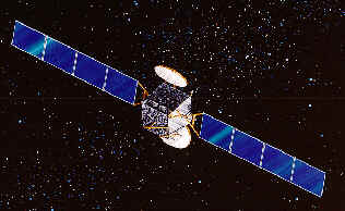
Compound Semiconductor devices are used for the solar panels and the RF transmitters and receivers in communications satelites (pictured is a DirecTV satelite by Hughes Electronics).
In the metalorganic chemical vapor deposition (MOCVD) process, volatile precursors, e.g., trimethylindium, trimethylgallium and phosphine, are fed to the reactor in hydrogen carrier gas. When these molecules flow over the hot substrate, they decompose and deposit a thin film, e.g., InGaP. By depositing a compound that is lattice matched to the substrate (e.g., GaAs (001)), an epitaxial single crystal is grown. A device is produced by varying the composition and doping in the layers, while maintaining lattice matching at all times.
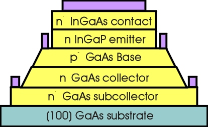
Heterojunction bipolar transistor (HBT) consisting of an n-type GaAs collector, p+ GaAs base, only 20 nm thick, and an InGaP emitter. These devices amplify RF signals by 20 times at a frequency of 1.9 GHz.
An example of a device grown by MOCVD is the heterojunction bipolar transistor (HBT) pictured above. This device is used extensively in digital cellular telephones and in high-speed communication networks. The critical layers in this device are only 10 to 20 nm thick. Thus, our research is at the cutting edge of Nanoscience and Technology.
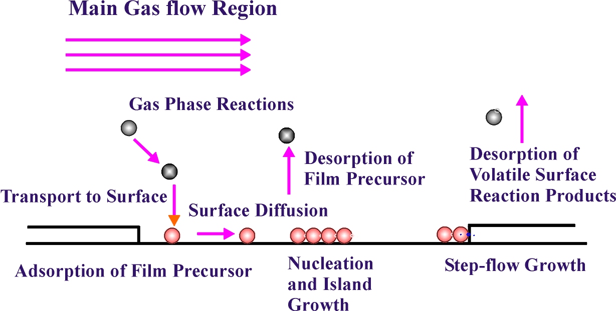
During MOCVD, a series of surface reactions occur as shown in the diagram below. These include adsorption and desorption of the precursor molecules, surface diffusion, nucleation and growth, and desorption of reaction products. In our laboratory, we characterize these surface reactions, and in particular, identify the sites on the semiconductor surface that mediate them. By understanding the atomic-scale processes that govern thin film growth, we make it possible to build new and more powerful devices.
At UCLA, the surface chemistry of MOCVD is revealed with state-of-the-art instruments, including reflectance difference spectroscopy, infrared spectroscopy, electron diffraction, x-ray photoemission, scanning tunneling microscopy, and ab initio molecular cluster calculations. Click on Facilities to learn more about our capabilities. In addition, you can check out some of the surfaces and surface sites that we have characterized by going to the STM Gallery and Molecular Clusters links, or by viewing our Publications.
Careers
Students working in this field learn all the skills necessary for rewarding careers in the microelectronics, communications, and high-tech materials industries. Our graduates are in great demand, and have landed exciting jobs with fast growing companies. You can see where our graduates have gone by clicking on Recent Graduates.