Scanning Tunneling Microscopy of III-V Compound Semiconductor Surfaces


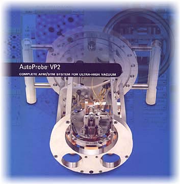
     In our facility, we have a Park Scientific scanning tunneling microscope/ atomic force microscope.  We have investigated the surface structures of many III-V compound semiconductors produced in the MOCVD reactor.  Some of the results are highlighted below.

bullet

Gallium arsenide (GaAs)

bullet

Indium arsenide (InAs) and Indium gallium arsenide (InGaAs)

bullet

Indium phosphide (InP) 

bullet

Arsenic-phosphorous exchange on indium phosphide (InP) 

bullet

Indium phosphide (111)A


© Copyright 1996-2007, R. F. Hicks, Semiconductor Material Chemistry and Plasma Processing Laboratory, University of California, Los Angeles.

For information, please contact Professor Robert F. Hicks
Last Modified May 21, 2007 05:58 PM