MULTI-FUNCTIONAL MATERIALS SYNTHESIS
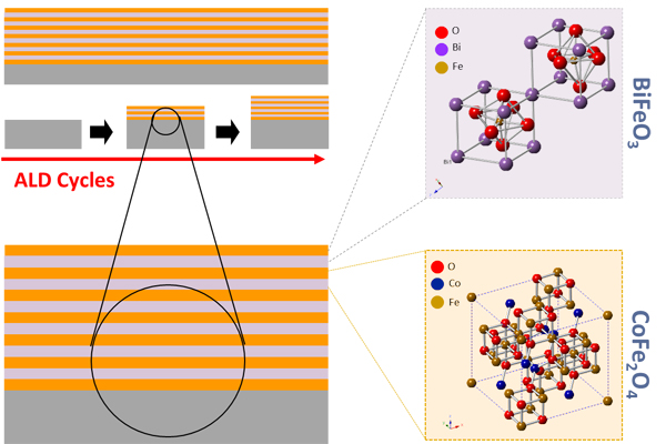
Atomic layer deposition (ALD) uses self-limiting reaction sequences to deposit atomic layer controlled thin films, ideal for tailoring the composition and microstructure of multi-functional materials for various applications.
MULTI-FUNCTIONAL MATERIALS PATTERNING
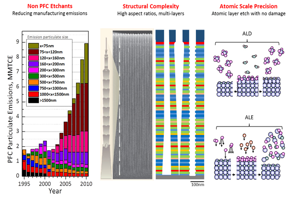
Plasma etching is the enabling technology that patterns thin film materials into high fidelity and specific structures for large scale integration. Atomic layer etching can be realized through the understanding and balance of specific surface reactions between ions and radicals.
3-D MICRO-BATTERIES & ENERGY STORAGE
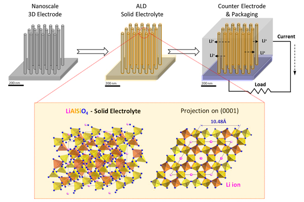
To rationally design an effective electrolyte material with a large contact area to the electrodes in miniaturized energy storage devices, ALD is used to synthesize metal oxide based electrolyte materials and understand the impact of structural properties on the attainable ionic conductivity.
FERROELECTRIC & WIDE BAND GAP MATERIALS
Multifunctional dielectric thin films are engineered and integrated on wide band gap semiconductors by ALD processing to enhance the functionalities of power electronics and radio frequency (RF) integrated circuits.
CORE-SHELL NANO PHOSPHORS
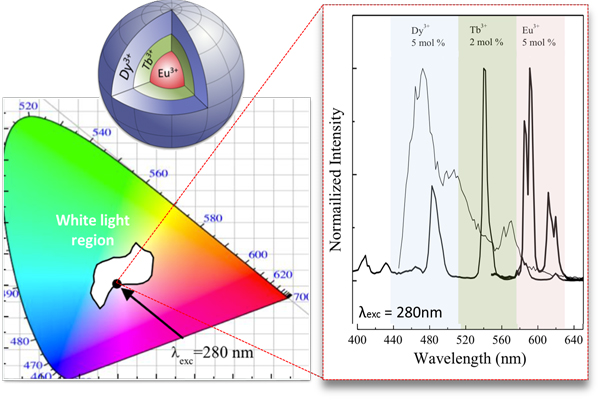
Core-shell rare-earth ion (RE) doped phosphors with spatially controlled dopants allow for the conversion of photons that are outside of the desired wavelengths into usable ranges for many applications such as in photovoltaics and for white light generation.
MULTI-FERROIC MATERIALS
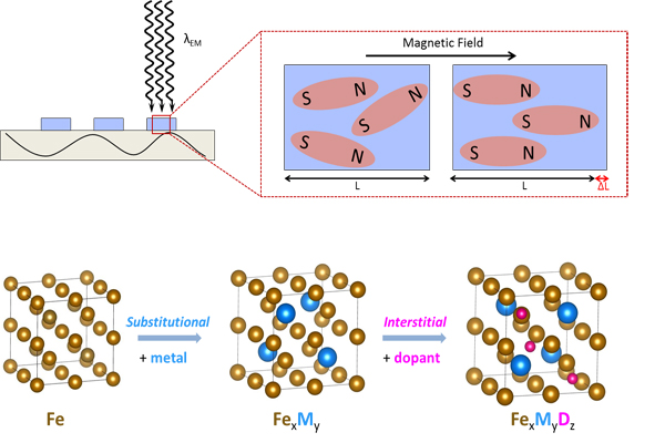
Doped, iron-based intermetallic materials are being developed for integration into composite multiferroic systems for RF applications.